SWIR Image Sensors

See the Unseen

Introduction

Outside of the typical visible light spectrum lies a range of longer wavelengths, the infrared range. This range is typically separated into four segments: Long Wave (LWIR) 8-12 µm, Mid Wave (MWIR) 3-5 µm, Short Wave (SWIR) 1.0-2.5 µm, and Near (NIR) 0.7-1.0 µm Infrared. The latter two are typically considered most similar to visible wavelengths with a light source and a target. The longer wavebands are emitted by objects due to their temperature. 

Though NIR and SWIR act similarly to visible light, they are not visible to the human eye. As a result, these spectrums present valuable information which can show artifacts or damage that would otherwise not be seen. Click here to see some examples of how SWIR is being used in existing applications today.  

Pixel Architecture

Many CMOS sensors are able to see into the NIR range with their standard architecture but cannot see into the SWIR range. These silicon sensors have an upper range limit around 1.0 µm. To look deeper into the SWIR range, InGaAs is used as a sensor material. It is a semiconductor grown with a specific ratio of (Indium, Gallium and Arsenic) giving it a spectral response of 1.1-1.7 µm. The typical drawback to these sensors is that they cannot see the shorter, visible color wavelengths due to the manufacturing process.  

For applications that want to see in both the visible and SWIR ranges, two sensors are needed to see these independently and then their images can be merged into one. This can be challenging to do as the cameras and captured images need to have similar fields of view, and optics being positioned very close to each other to minimize any disparity. This process often has alignment issues in the final images that make them difficult to get the best results for a given application. New technology and sensor substrates are being developed that are making it possible to overcome these challenges with only a few drawbacks or sacrifices.  

Sony’s SenSWIR Technology 

The demand for higher productivity is driving the growing interest in image capture in both the visible spectrum and SWIR wavelengths. SenSWIR from Sony can capture wavelengths from 0.4 – 1.7 µm allowing one image sensor to see both the visible and SWIR spectrums of light simultaneously. For this reason, the market trend for SWIR sensors is promising and technical developments are progressing rapidly. Do you already know SenSWIR? 

Sony’s SenSWIR technology, leverages Sony’s semiconductor processing and their copper-to-copper connection producing smaller pixels, not otherwise available with InGaAs sensors. As a result, smaller high-resolution cameras can be developed, which can support higher inspection precision. 

Image Source: https://www.sony-semicon.co.jp/e/products/IS/industry/technology/swir.html

Discover several ways to benefit from Sony’s first-class SWIR solutions

The demand for higher productivity is driving the growing interest in image capture in both the visible spectrum and SWIR wavelengths. For this reason, the market trend for SWIR sensors is promising and technical developments are progressing rapidly. 

Under visible light

Under SWIR imaging conditions

Image Source: https://www.sony-semicon.co.jp/e/products/IS/industry/technology/swir.html

Explore the advantages in a variety of applications

Sorting of Products

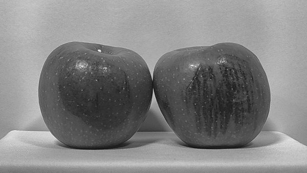
Ideal for applications such as sorting fruits and vegetables, as light in the SWIR band enables detection of moisture content, which is difficult to determine under visible light.

Foreign Material Inspection

Properties of light absorption and reflection in SWIR imaging are applied to distinguish substances that would be difficult to differentiate under visible light alone.

Semiconductor Inspection

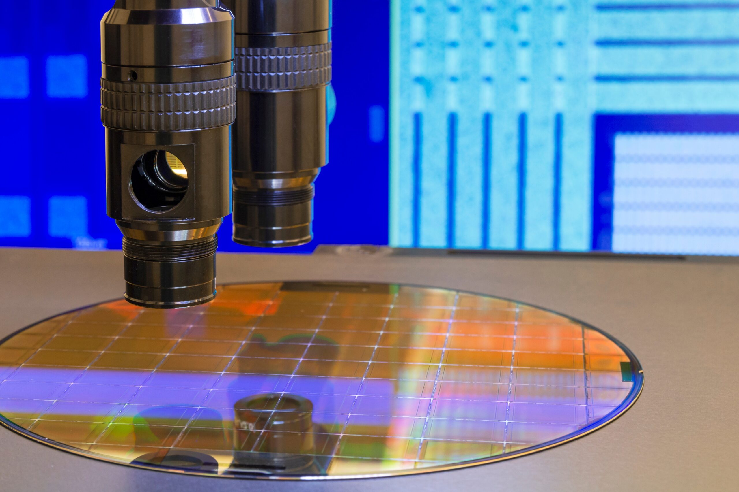
Light in the SWIR band passes through material made of silicon. This aspect of SWIR imaging is applied in semiconductor production and inspection.

Temperature Estimation

Around hot objects, light in the SWIR band shines quite brightly. Temperature can be estimated from differences in brightness among several wavelengths. This is used to estimate the temperature of welds or other hot areas.

Remote Observation

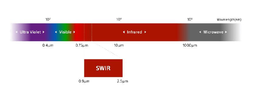
Light in the SWIR band has longer wavelengths than visible light. This makes the light less susceptible to scattering, thus apply SWIR imaging successfully in remote observation.
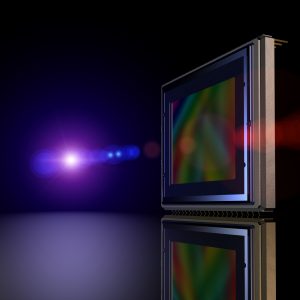
Learn more details about the possibilities provided by Sony’s SWIR technology

In IMX990 and IMX991, SenSWIR technology has enabled Sony to overcome challenges in pixel miniaturization to offer sensors that are compact, high-resolution, and capable of imaging from the visible spectrum to SWIR wavelengths.

The advances in performance and functionality introduced by the IMX990 and IMX991 pave the way for the development of SWIR industrial cameras and inspection equipment for a diverse range of applications such as inspection, identification, and measurement. 

Sensors

Sony IMX991-AABJ-C
Sony CMOS Global shutter SWIR, 0.34 MP, 656 x 520, 1/4 inch, 5 x 5 µm, 240 fps, SLVS, LGA (Ceramic) TEC less,
Sony IMX991-AABA-C
Sony CMOS Global shutter SWIR, 0.34 MP, 656 x 520, 1/4 inch, 5 x 5 µm, 240 fps, SLVS, PGA (Ceramic) TEC | with built-in...
Sony IMX990-AABJ-C
Sony CMOS Global shutter SWIR, 1.34 MP, 1296 x 1032, 1/2 inch, 5 x 5 µm, 120 fps, SLVS, LGA (Ceramic) TEC less,
Sony IMX990-AABA-C
Sony CMOS Global shutter SWIR, 1.34 MP, 1296 x 1032, 1/2 inch, 5 x 5 µm, 120 fps, SLVS, PGA (Ceramic) TEC | with built-in...

Evaluation Kits

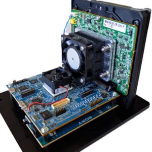
Sony IMX991-AABJ EVB-Kit
Sensor evaluation kit, Sony, 0.34 MP, monochrome, Uncooled PKG | Includes IMX990EVB-DBF, IMX990EVB-MCB, IMXEVB-CUE3S and a sensor
Sony IMX991-AABA EVB-Kit
Sensor evaluation kit, Sony, 0.34 MP, monochrome, Cool PKG | includes: IMX990EVB-DAF, IMX990EVB-MCA, IMXEVB-CUE3S and a sensor
Sony IMX990-AABJ EVB-Kit
Sensor evaluation kit, Sony, 1.31 MP, monochrome, optics: C, Uncooled PKG | Includes IMX990EVB-DBF, IMX990EVB-MCB, IMXEVB-CUE3S and a sensor
Sony IMX990-AABA EVB-Kit
Sensor evaluation kit, Sony, 1.31 MP, monochrome, optics: C, Cool PKG | includes: IMX990EVB-DAF, IMX990EVB-MCA, IMXEVB-CUE3S and a sensor

LET US ANSWER ANY QUESTIONS YOU HAVE ABOUT IMAGE SENSOR TECHNOLOGIES OR REQUEST A SAMPLE TODAY.