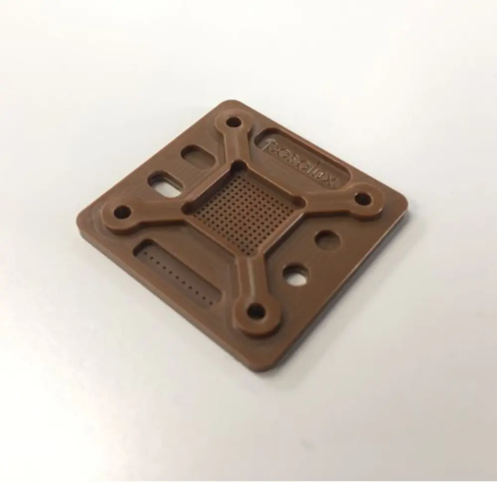
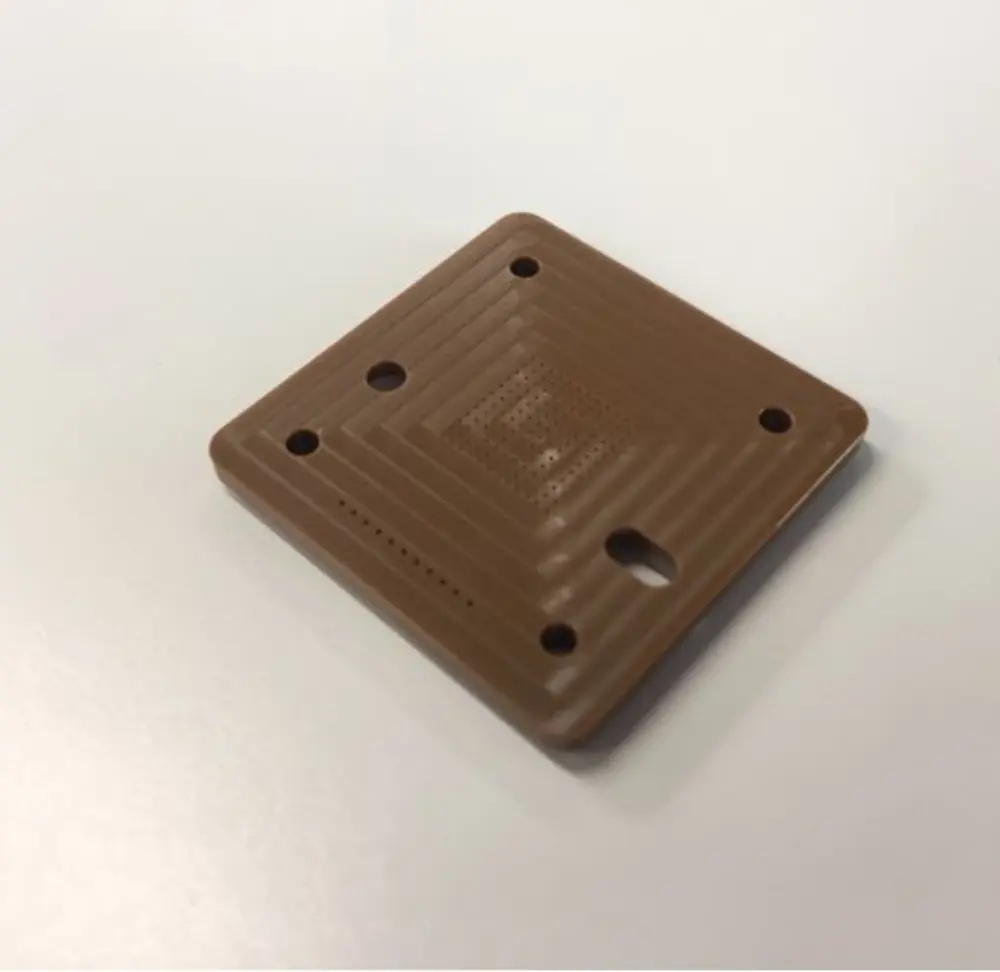
Test socket guide plates micro machining (drilling, milling cutting) for semiconductors testing industry
Adapting to swift semiconductor advancements, the micromachining processes must ensure adaptability without compromising speed and accuracy.
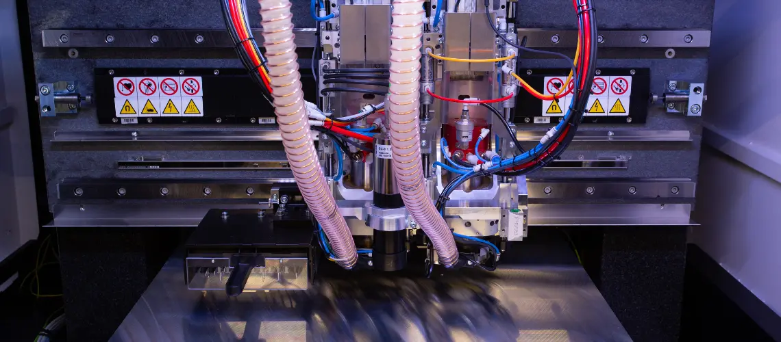
Test socket guide plates micromachining application overview
Test socket guide plates micromachining represents the pinnacle of high-tech precision in the semiconductor testing landscape. Harnessing advanced techniques, this application seamlessly navigates the intricate geometries of cutting-edge semiconductor architectures. In a world where nanometers make a difference, micromachining emerges as the avant-garde solution, ensuring flawless alignment and impeccable testing fidelity in an ever-evolving tech-driven world.
Test socket guide plates micro-machining results and achievements
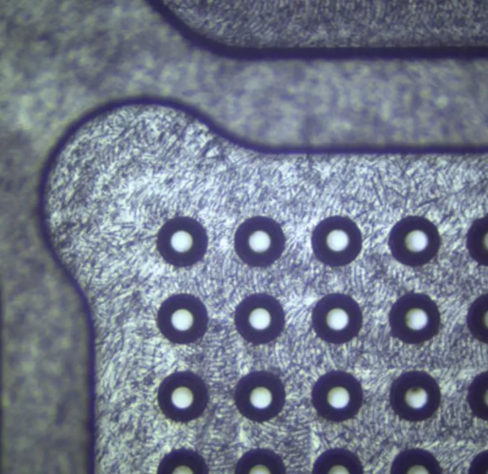
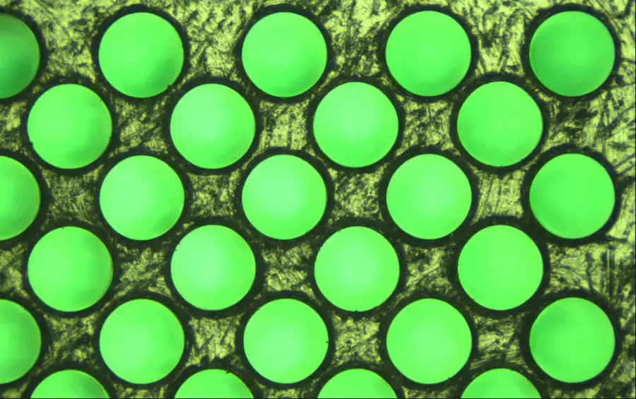
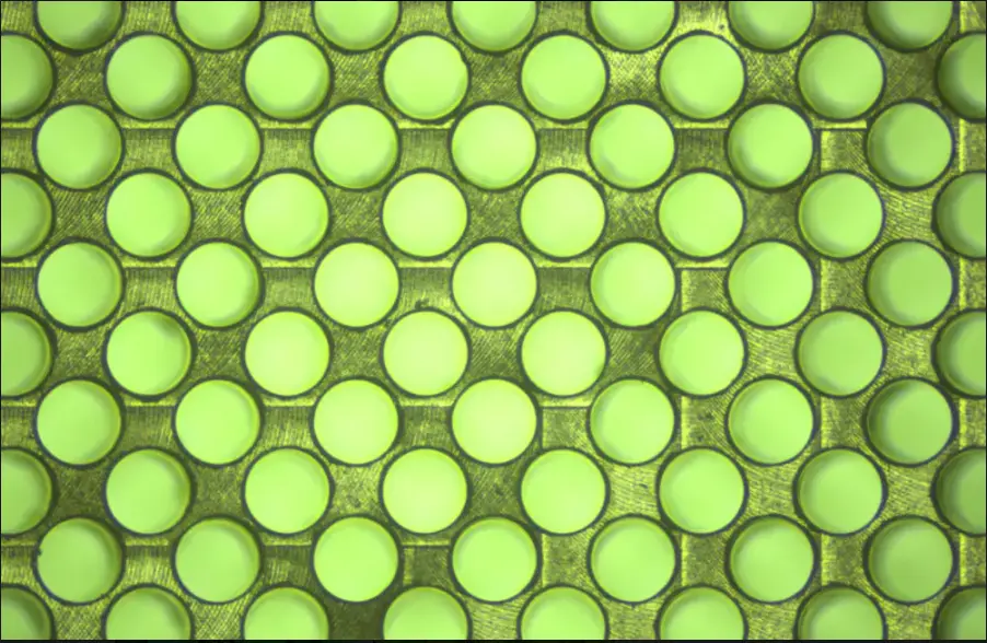
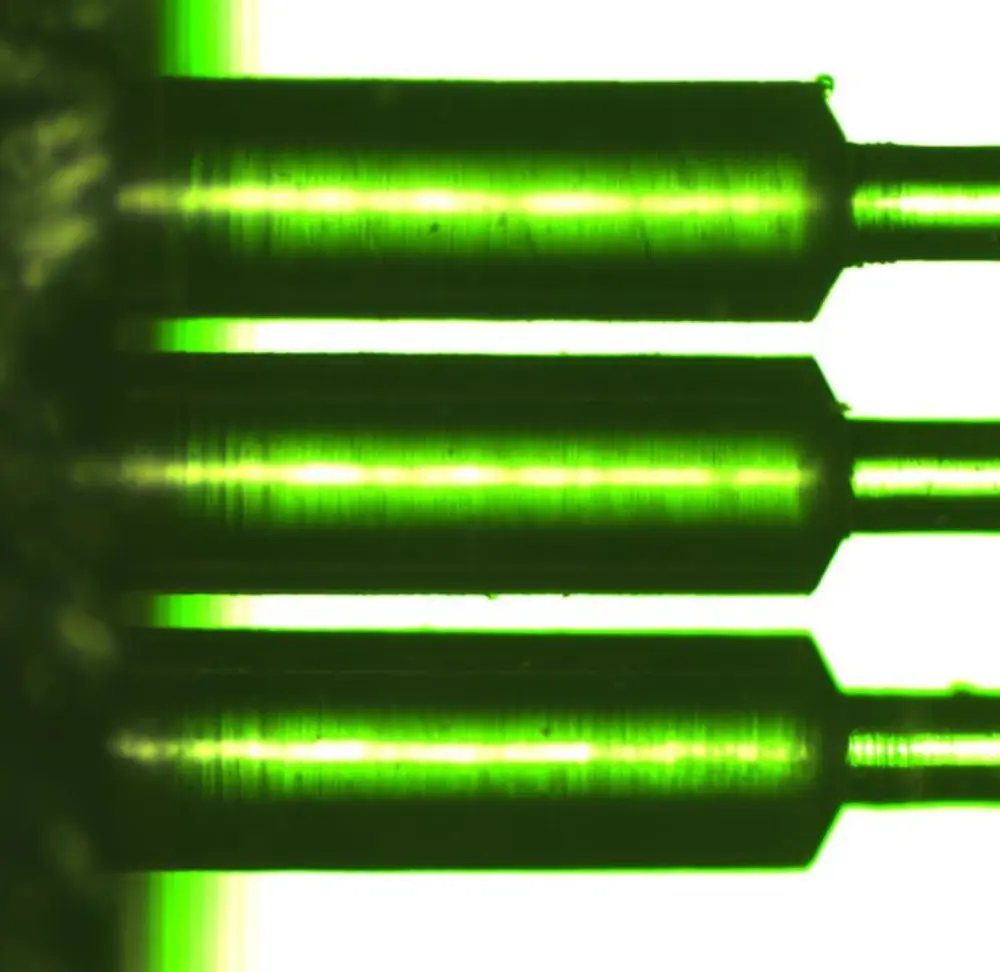
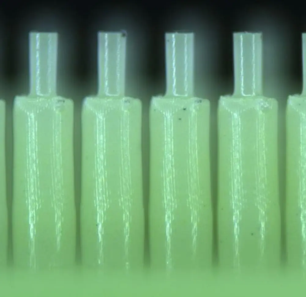


Precision we can achieve
Round holes of Ø 300 μm are milled with a 350 μm pitch into both Torlon and Vespel materials, featuring a 500 μm thickness and an impressively swift cycle time of 0.6 seconds. Torlon also accommodates a countersunk step hole, precisely measured at Ø 3.0 mm with a 1 mm depth and Ø 2.5 mm with a 0.8 mm depth. In contrast, Vespel showcases the expertise with step holes from Ø 400 μm down to 650 μm, set at a pitch of 750 μm, and through holes meticulously drilled to Ø 200 μm and a depth of 650 μm.
You currently have a test socket guide plate micromachining project and you would like to know what we could achieve together?
Give us some more details!
Mechanical micromachining, commonly known as micromachining, is a specialized manufacturing technology that involves the use of micro tools, such as micro-endmills or drillbits, with geometrically defined cutting edges. This subtractive fabrication process crafts devices or features with dimensions in the micrometer range. It mirrors traditional machining in approach but operates on a distinctly smaller scale, necessitating specialized equipment and techniques to define microscale structures or components. Mechanical micromachining provides:
- Flexibility
- Cost-effective solution for small-batches
- Complex geometry
- Reduced waste
- Integration
- Scalability
- Direct production

The ULTIMATE machines are innovative, fully-automated, 4-axis micromachining centers for high-speed drilling and milling. Our advanced mechanical µ-machining solution for your high-tech production.
Other applications that might be interesting for you

Turning of contacts pins for IC substrates testing industry
Turning of contact pins (wires, bars and tubes) for semiconductors testing industry
Drilling and routing of composites and non-ferrous materials for printed circuit boards (PCB) industry
Let’s discuss your micro-machining operations
If you are looking for a high-tech production system as well as a partner to process state-of-the-art micro-machining, you are in the right place.