- Offer Profile
- Hamamatsu has been working with the Photon for more than 50 years. We have established ourselves as the top company of photoelectron conversion technologies in the world. However, we have yet to fully grasp the nature of the Photon and its potential. The more you study, the more you realize how little you know about the Photon and its applications. That is why we continue to move ahead vigorously with basic research and apply what we learn to photonics.
Photoelectron conversion technologies
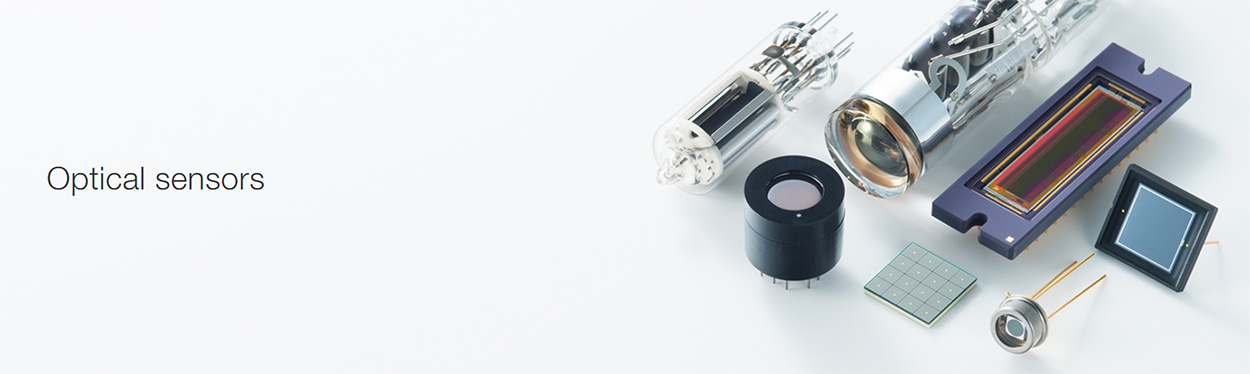
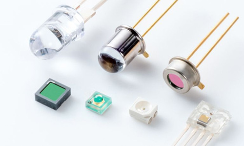
Optical sensors
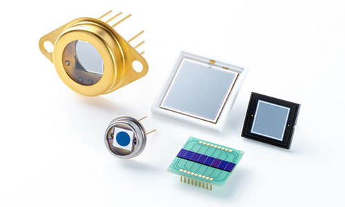
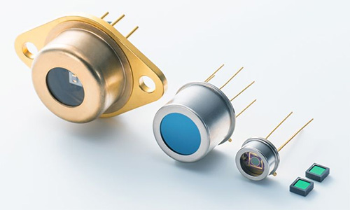
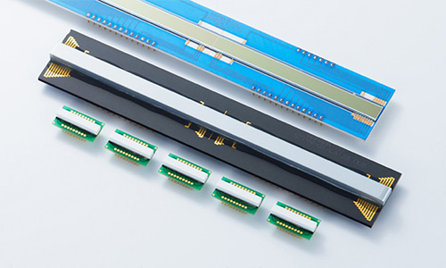
Photodiodes
-
Our photodiodes cover a broad spectral range, from near-infrared and ultraviolet wavelengths to high-energy regions. Photodiodes are available in metal, ceramic, and plastic packages, as well as module types. Custom designs are also available.
- Si photodiodes
- Si photodiode arrays
- Si photodiode arrays with amplifier
- InGaAs photodiodes
- InGaAs photodiode arrays
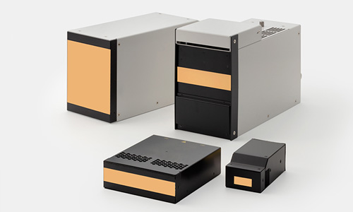
- Photodiode modules
- Photosensor amplifiers
- Optics modules
- Balanced detectors
- Charge amplifiers
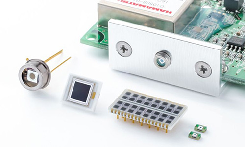
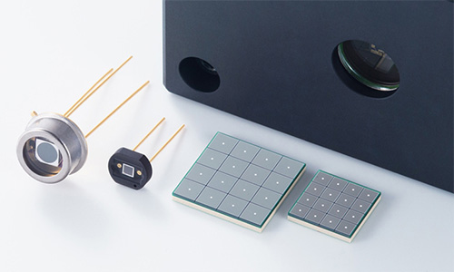
Avalanche photodiodes (APDs)
-
APDs are photodiodes with internal gain produced by the application of a reverse voltage. They have a higher signal-to-noise ratio (SNR) than PIN photodiodes, as well as fast time response, low dark current, and high sensitivity. Spectral response range is typically within 200 - 1150 nm.
- Si APDs
- InGaAs APDs
- Si APD arrays
- APD modules
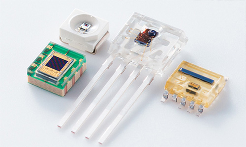
Photo IC
-
The photo IC is an intelligent optical sensor with diverse functions and integrates a photodiode with signal processing IC in the same package.
- Photo IC for rangefinders
- Front-end IC photosensors for LiDAR
- Color sensors
- Illuminance sensors
- Schmitt trigger circuit photo IC
- Light modulation photo IC
- Photo IC for optical link
- Photo IC devices for encoders
- Photo IC for optical switch
- Photo IC for laser beam synchronous detection
Multi-Pixel Photon Counters (MPPCs/SiPM)
-
Our Multi-Pixel Photon Counter (MPPC), also known as silicon photomultiplier (SiPM), is a solid state photomultiplier comprised of a high density matrix of Geiger-mode-operated avalanche photodiodes also known as SPAD (single-photon avalanche photodiode). These SPADs have high internal gain which enable single photon detection. The Hamamatsu SiPM features low dark count, high photon detection efficiency, excellent timing resolution, low bias voltage operation, ruggedness, resistance to excess light, and immunity to magnetic fields. They are well-suited to single photon counting and other ultra-low light applications.
- MPPCs (SiPMs)/MPPC arrays
- MPPC modules
- Single-pixel photon counting modules
- MPPC power supplies & driver circuits
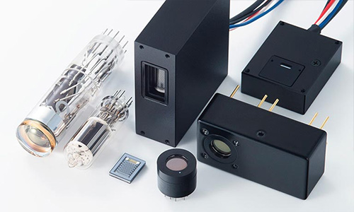
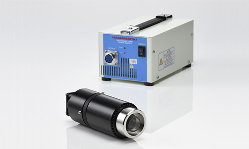
Photomultiplier tubes (PMTs)
-
PMTs suitable for applications that require high speed, low noise, and high gain. Our PMTs include bare tubes, assemblies, and modules offering a wide selection of photosensitive areas and spectral responses.
- Photomultiplier tube (Tube alone)
- Photomultiplier tube assemblies
- Photomultiplier tube modules
- Micro PMTs
- Photomultiplier tube accessories
- Photon detection units
- Hybrid photodetectors (HPDs)
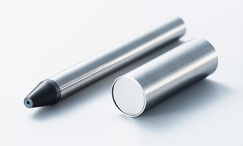
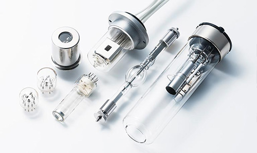
Phototubes
- Phototubes are photodetectors that feature high sensitivity, superior temperature stability, wide dynamic range, large photosensitive area, and low-voltage operation. They are widely utilized in applications such as chemical and medical analysis and laser measurement.
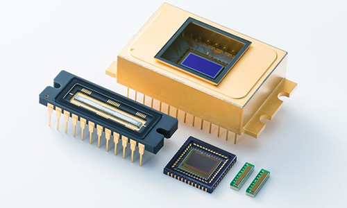
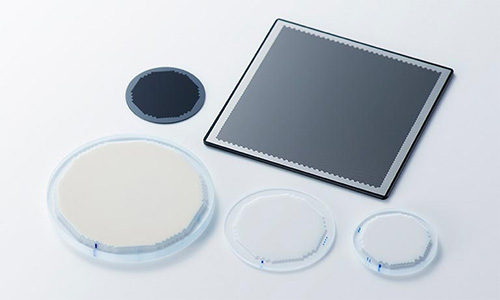
Image sensors
- We offer over 200 standard linear and area image sensors covering the short wavelength infrared (SWIR), near infrared (NIR), visible (VIS), ultraviolet (UV), and X-ray regions. With a broad selection from high speed, high sensitivity to wide dynamic range, our image sensors are suitable for different applications including spectroscopy analysis using spectrometers, industrial imaging such as machine vision cameras, microscopy, and distance measurements. We also provide supporting electronics such as easy-to-use driver circuits for sensor evaluation and driver modules for OEMs. Customizations are available for specific applications and requirements.
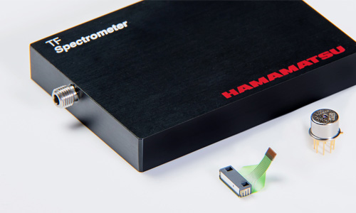
Spectrometers / Spectrum sensors
-
- Mini-spectrometers: Mini-spectrometers are compact and low cost spectrometers (polychromators). We offer over 20 different types of mini-spectrometers covering the spectral range from UV to NIR. Suitable for applications such as environmental measurement, color measurement, quality control in production lines, and information devices.
- MEMS-FPI spectrum sensors: Ultra-compact sensors that house an InGaAs PIN photodiode and a Fabry-Perot Interferometer (MEMS-FPI) tunable filter that can vary its transmission wavelength depending on the applied voltage.
- Raman spectroscopy: Our modules include all the essential components needed to perform Raman measurements, such as excitation laser diode, polychromatic dispersion device, and optical and control circuit systems.
Infrared detectors
-
Sensors and modules for infrared light detection:
- InGaAs photodiodes
- InGaAs photodiode arrays
- InGaAs APDs
- Thermopile detectors
- InAs photovoltaic detectors
- InAsSb photovoltaic detectors
- InSb photoconductive detectors
- InSb photovoltaic detectors
- Two color detectors
- Photon drag detectors
- Infrared detector modules with preamplifier
- Infrared photodiode modules
UV & flame sensors
-
- Discharge / Flame sensors UVTRON
- UV power meters
- Photo IC assemblies for flame detection
- Thermopile detectors
- InAsSb photovoltaic detectors
X-ray sensors
-
Sensors and modules for x-ray detection.
- Si photodiodes
- Si photodiode arrays
- Si photodiode arrays with amplifier
- X-ray flat panel sensors
- X-ray image sensors
- X-ray TDI cameras
- X-ray line scan cameras
- Scintillator plates
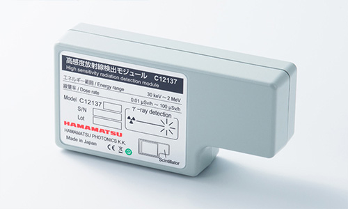
Radiation sensors
- Sensors and modules for radiation detection.
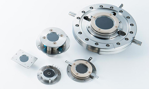
Electron & ion sensors
-
- Fast decay phosphors
- Electron multipliers (EMs)
- Microchannel plates (MCPs)
- Photodiodes for electron beam detection

Distance & position sensors
-
Sensors used for distance measurement and position detection. Suitable for many applications, such as LiDAR.
- LiDAR sensors
- Photo IC for rangefinders
- Distance image sensors
- Position-sensitive detectors (PSDs)
- Profile sensors
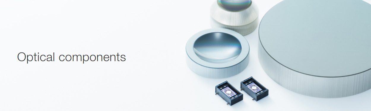
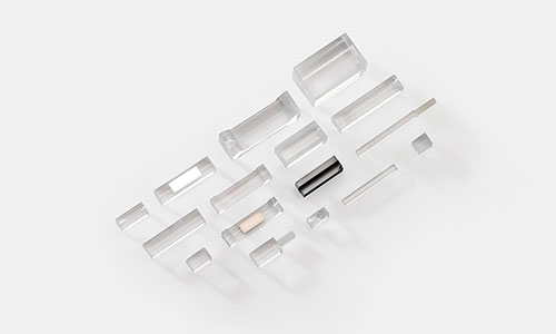
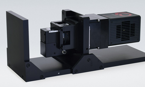
Optical components
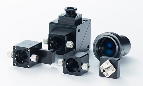
Optical blocks
- Compact units containing optical components such as bandpass filters and dichroic mirrors. Designed specifically for low light level measurements that use PMT modules and high-sensitivity cameras. Can be combined in different configurations. A full system can be built by combining these blocks with a light source and detector. For example, a low cost fluorescence or confocal microscope can be built by combining a laser, optical blocks, and microscope objective lenses.
Fiber optic plates (FOP)
- Optical devices comprised of a bundle of micron-sized optical fibers. Used as a lens to transmit light or an image with high efficiency and low distortion. Unlike a normal optical lens, no focusing distance is required. Ideal when designing and building compact optical devices.
Terahertz wave plate
- This is a Fresnel rhomb wave plate for controlling terahertz wave polarization. The adoption of Fresnel rhomb makesit possible to handle a terahertz wave over a broad band.
FAC lenses
- FAC lenses collimate diverging light from a semiconductor laser into a narrow beam with a radiation angle of several milliradians (mrad) or less, to allow efficient use of light.
Collimating capillary lenses
- Capillary lenses collimate x-rays using total reflection. They consist of a bundle of numerous hollow glass capillaries formed into a cylindrical shape with one end gently tapered.
Capillary plates
- Circular or square glass plates ranging from 0.4 to several dozen millimeters thick with fine glass tubing (capillaries) regularly arranged in a two-dimensional array. Each capillary hole can be from a few microns to several hundred microns in diameter. These plates have excellent linearity and high precision while offering selectable directivity, making them suitable for flow control and particle sorting.
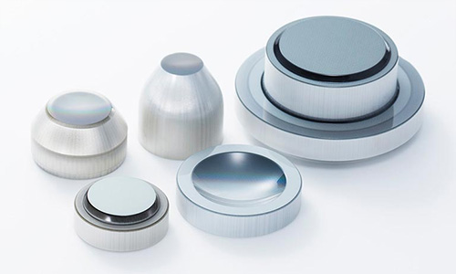
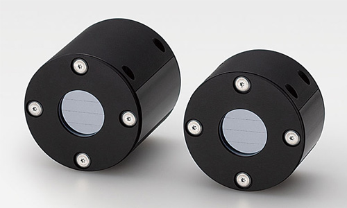
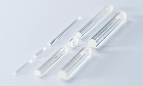
Flow cells
- Quartz glass flow cells and cuvettes manufactured using our experience and established glass processing technology. We also provide custom-made products.
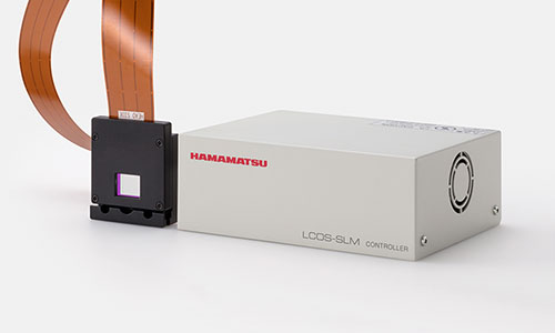
LCOS-SLM (Optical Phase Modulator)
- LCOS-SLM are reflective space light phase modulators that freely modulates light phases. Laser or other irradiation light goes through a phase modulation by the liquid crystal and reflected. The wavefront shape can be controlled freely. Wavefront control of the light can be applied to optical beam photolithography, aberration correction, and the like.
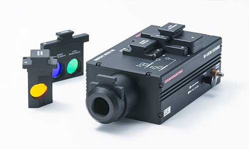
Image splitting optics
-
Image splitting optics provide one pair of dual wavelength images to cameras.
- The W-VIEW GEMINI-2C is an image splitting optics which provides one pair of dual wavelength images separated by a dichroic mirror onto two cameras.
- The W-VIEW GEMINI is an image splitting optics which provides one pair of dual wavelength images separated by a dichroic mirror onto a single camera.
MEMS mirrors
- Electromagnetically driven mirrors that incorporate our unique micro-electro-mechanical systems (MEMS) technology. They offer a wide optical deflection angle, high mirror reflectivity, and low power consumption.
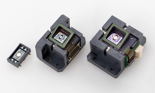
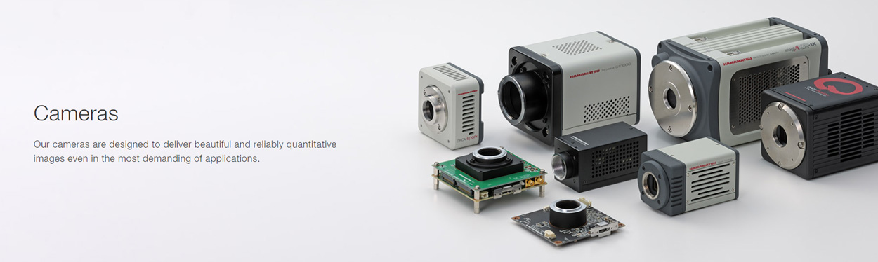
Cameras
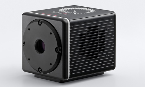
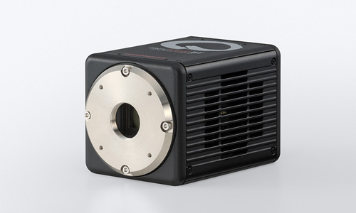
qCMOS cameras
-
The world's first camera to incorporate the qCMOS image sensor. The camera achieves the ultimate in quantitative imaging.
Groundbreaking in concept and unprecedented in performance.
Since the 1980s, Hamamatsu Photonics has continued to develop high-sensitivity, low-noise cameras using its unique camera design technology and has always contributed to the development of cutting-edge scientific and technological research. Now, we are proud to release the ORCA-Quest with ultimate performance. The C15550-20UP is the world's first camera to incorporate the qCMOS image sensor and to be able to resolve the number of photoelectrons using a newly developed dedicated technology. The camera achieves the ultimate in quantitative imaging.
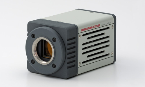
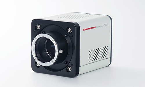
CMOS cameras
-
A leader in the scientific CMOS camera revolution, Hamamatsu has a camera to fit almost any budget or application.
- The ORCA-Fusion, built from the sensor up, balances the complex nuances of camera features to provide beautiful images and robust data at all lights levels, but especially in tough low-light conditions.
- The ORCA-spark is a high-sensitivity digital CMOS camera using a 2.3 megapixel CMOS sensor.
- Second generation CMOS camera with sCMOS sensor designed for scientific research use. The ORCA-Flash4.0 LT+ is designed to be the new workhorse digital camera to bring high end performance to every imaging project. (Peak QE: 82 %)
- Digital CMOS camera with sCMOS sensor designed for scientific research use. It has improved resolution and sensitivity (especially in NIR region) comparing with ORCA-Flash4.0. (82 % peak QE)
InGaAs cameras
-
InGaAs cameras bridge the gap between NIR wavelengths in the 950-1700 nm range, where silicon detectors are no longer sensitive. Our products capture images with QVGA to VGA resolution and our extensive experience with InGaAs sensors allows us to offer cameras with exquisite image contrast and quality.
- Infrared sensitive InGaAs camera with detection range from 950nm to 1700nm. It supports standard video output USB 3.0.
- Infrared sensitive InGaAs camera with detection range from 950nm to 1500nm. Low dark current with -70 °C peltier cooling.
- Infrared sensitive InGaAs camera with detection range from 950nm to 1700nm. It supports standard video output (EIA) and USB 3.0.
TDI camera
-
High-speed imaging of moving samples is a challenging even in bright conditions, but our TDI cameras turn linear movement of the sample into an advantage by coordinating signal accumulation in the sensor with sample movement. These cameras are also well-suited for low-light scanning applications that are too dim to for a line scan sensor.
- TDI (Time Delay Integration) camera with 2048 horizontal pixel. It realizes high speed and high sensitivity simultaneously and is good for variety of applications including in-line use.
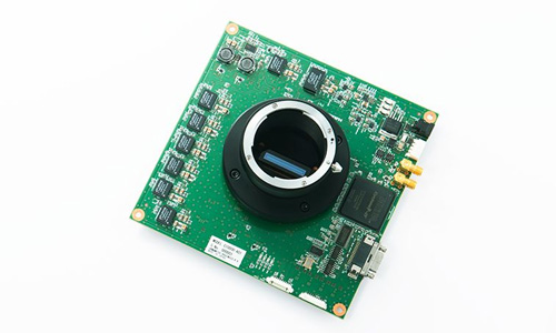
Board level cameras
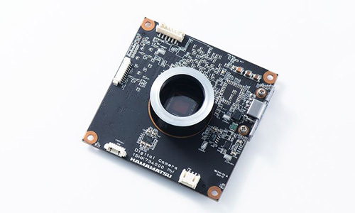
Board-level CMOS cameras
- While our board-level CMOS cameras use the same sensors as our CMOS cameras for research, their streamlined features deliver high speed, low noise, and high resolution at a cost-effective price.
Board-level TDI cameras
- From our fast, low-noise TDI sensors to advanced camera engineering capabilities that optimize sensor performance, these board-level cameras allow you to harness decades of in-house design and manufacturing experience in your next OEM project.
X-ray cameras
X-ray line scan cameras
- X-ray line scan cameras produce high-sensitivity, high-resolution, X-ray transmission images of moving objects transported on a conveyor belt or similar apparatus. A variety of options are available.
X-ray TDI cameras
- Cameras useful for in-line imaging applications requiring high-speed operation with high sensitivity. While conventional line sensor cameras suffer from low brightness under high-resolution imaging, X-ray TDI cameras improve the image brightness, resulting in enhanced images. Most appropriate for imaging linearly moving objects or where the aspect ratio is significantly asymmetric. Vertical X-ray TDI cameras that can be installed in narrow spaces are also available.
X-ray CMOS cameras
- X-ray CMOS cameras are suitable for micro object by achieving high resolution image.
X-ray I.I. camera unit & X-ray I.I.
- X-ray camera units those contain an X-ray image intensifier and a CCD camera.
High resolution X-ray imaging system
- High-resolution imaging system designed for X-ray beam alignment. Suitable for use in larger synchrotron radiation facilities.
Software
Imaging software
- Software provides the interface to access all our carefully engineered camera features, from simply setting exposure to orchestrating complex triggering for multidimensional experiments. Not only are our cameras supported by most imaging platforms, we also offer software development tools for Windows, Linux, MATLAB and LabVIEW.
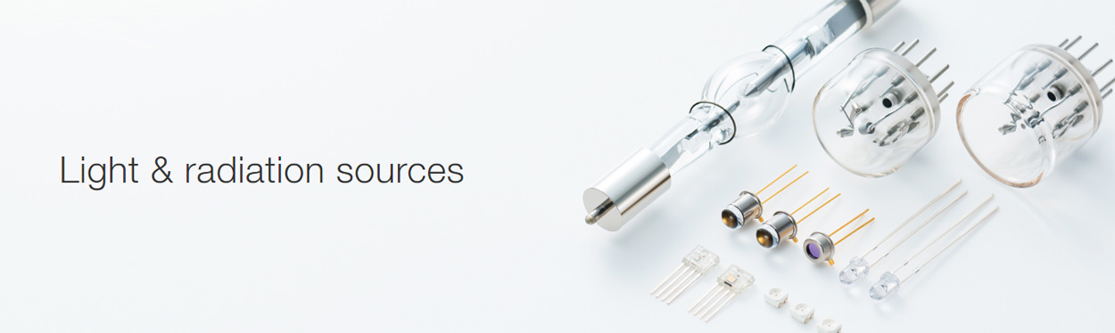
Light & radiation sources
LEDs
- Our LEDs range from red to mid-infrared, a variety of wavelengths enabled by crystal growth and process technology that supports compound semiconductor materials. LEDs are mainly used in combination with photosensors, and offer a lower cost and longer service life compared to laser diodes. High quality and reliability are ensured by strictly controlled assembly and inspection processes.
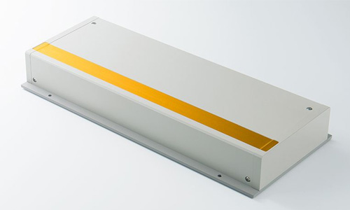
UV-LED light sources
-
Light sources available in a variety of intensities, cooling methods, and shapes. Suitable for a diverse range of applications, including UV adhesive curing and UV ink drying.
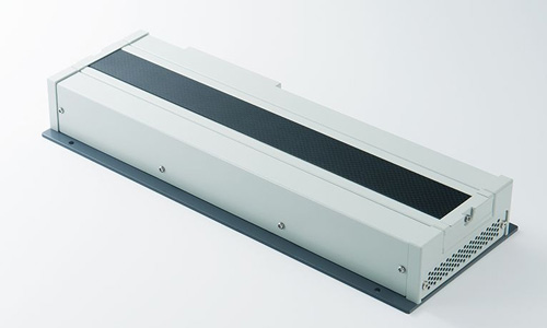
- UV-LED light source (Linear irradiation)
Hamamatsu now offers LED-UV light sources that are compact, lightweight and air-cooled, yet deliver the high power that has been a challenge for LED-UV light sources. These LED-UV light sources are available for various printers including inkjet printers. - Spot irradiation UV-LED light sources
Reduce costly down time due to lamp replacement with 365 or 385 nm UV-LED light sources.
- UV-LED light source (Linear irradiation)
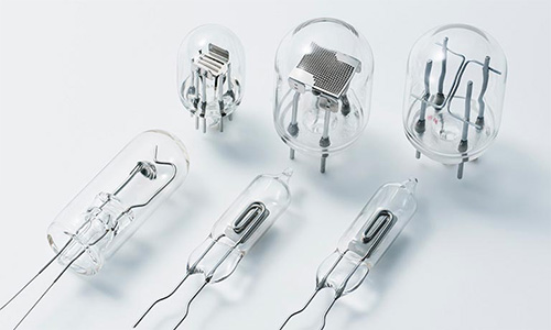
Lamps
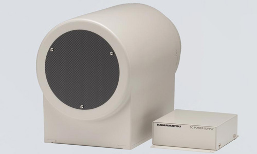
-
Our lamps deliver high stability and long lifetimes. Light measurement technology is utilized in many applications including chemical analysis, medical diagnostic testing, environmental monitoring, and academic research fields.
- Xenon & mercury-xenon lamps
- Xenon flash lamps
- Deuterium lamps
- Deuterium lamps for photoionization
- Hollow cathode lamp
Lamp modules & units
-
Our lamp modules and lamp units are assembled with a matching power supply and other functions making them suitable for a wide range of user applications.
- Xenon flash lamp modules
- Spot light sources
- Radio frequency (RF) electric discharge type excimer lamp
- Compact D2 lamp modules
- H2D2 light source units
- VUV light source units
Microfocus X-ray sources
- Microfocus X-ray sources specifically developed for 2D and 3D nondestructive testing. A small focal point prevents blurring of x-ray images and delivers a sharp, enlarged image.
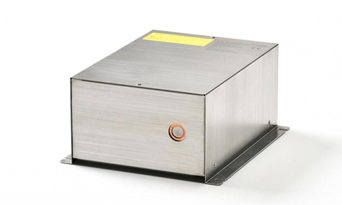
Soft X-ray source
- The high-stability soft X-ray source assembled with a power supply in a compact module.
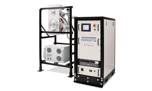
Extreme Ultraviolet (EUV) and Soft X-Ray Sources
- EnergetiqÂs Electrodeless Z-Pinch technology has excellent spatial stability, and stable repeatable power output.
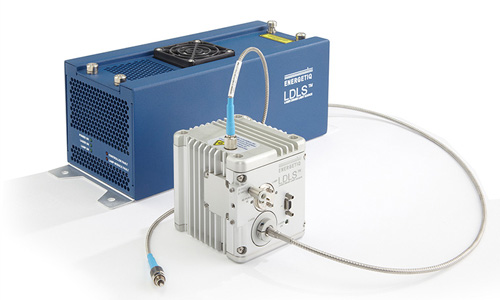
Laser-Driven Light Sources
- Energetiq has developed a revolutionary single-lightsource technology called the LDLSÂ Laser-Driven Light Source that enables extreme highbrightness over a broad spectral range, from 170nm through visible and beyond.
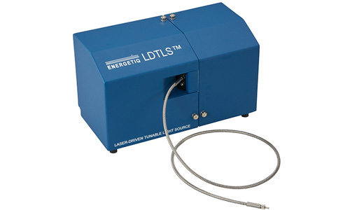
Laser-Driven Tunable Light Sources
- The Laser-Driven Tunable Light Source (LDTLSÂ) is a compact, fully integrated and highly stable tunable broadband light source based on proven Laser-Driven Light Source (LDLSÂ) technology.

Excimer la,p light sources
- Excimer lamp light sources contribute to surface modification, dry cleaning, oxidative decomposition, TOC measurement, and VOC decomposition. The optimum product can be selected based on the product size and irradiation area.
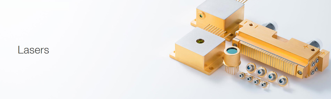
Lasers
Semiconductor laser
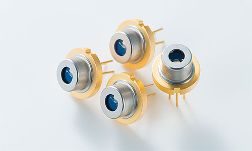
CW laser diodes (CWLD)
- These LDs are designed to be driven in continuous wave (CW). Output power is from mW to a few W.
Pulsed laser diodes (PLD)
- These LDs feature high peak power under pulsed operation. Various types are available with different peak output power and emission widths. These LDs can be used for distance measurements such as laser radar, hazard monitoring in security applications, etc.
Super luminescent diodes (SLD)
- SLDs combine the high brightness of laser diodes with the low coherence of LEDs. Suitable for optical applied measurements and medical imaging.
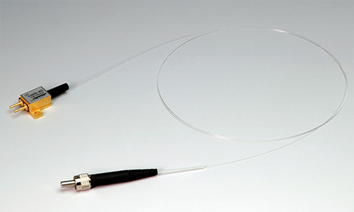
Fiber output laser diodes
- Fiber-coupled laser diodes are built using high power laser diodes in compact, hermetically sealed packages.
Quantum cascade lasers (QCL)
- Quantum cascade lasers are semiconductor lasers that offer peak emission in the mid-IR range (4 μm to 10 μm). These devices are an excellent light source for mid-IR applications, such as molecular gas analysis and absorption spectroscopy.
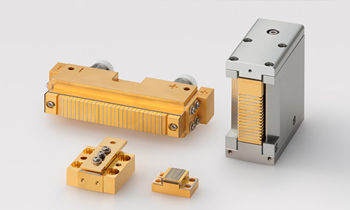
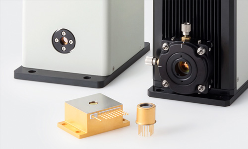
High-power laser diode bar modules
- With their emitting areas arranged in line to make a linear array, LD bar modules achieve high performance, high output power, and high reliability when coupled with appropriate cooling devices.
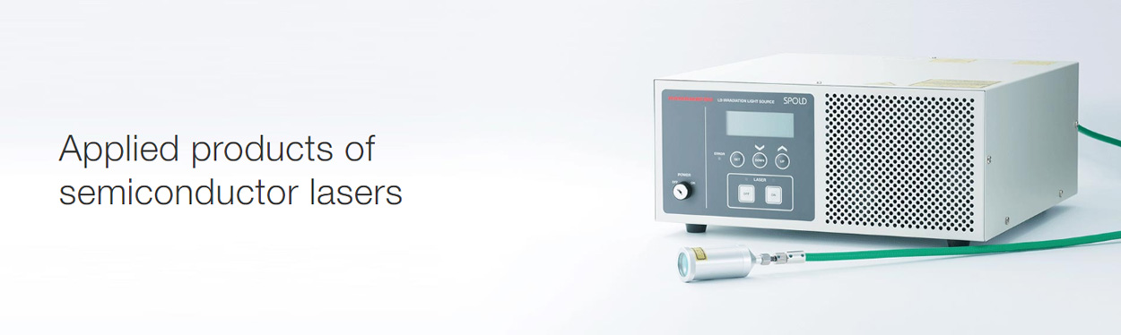
Applied products of semiconductor lasers
Laser heating system
- This is a laser heating system equipped with a temperature measurement function. It is effective for high precision and high reproducibility of laser heating process.
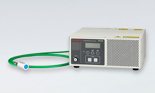
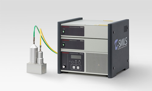
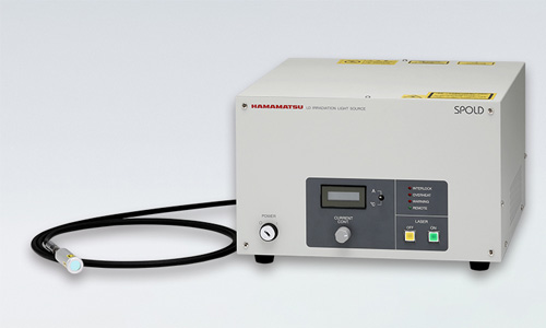
LD irradiation light sources (SPOLD)
- LD irradiation light source (SPOLD) is the lightweight & compact spot laser light source suitable for mounting into equipment.
SPOLD built-in process monitor
- The bult-in monitoring function allows “visualization” of laser processing that is deal for setting processing conditions and for checking reproducibility.
Solid state lasers
- Solid state laser products developed by merging our optical design technology, optical thin film technology, MEMS (Micro-Electro-Mechanical-Systems) and optical nanoscale technology and other cutting-edge technologies.
Pulsed solid state lasers
- This pulsed solid state laser is suitable for industrial applications due to its excellent stability and maintainability.