- Offer Profile
Renesas Electronics Corporation delivers trusted embedded design innovation with complete semiconductor solutions that enable billions of connected, intelligent devices to enhance the way people work and live.
A global leader in microcontrollers, analog, power, and SoC products, Renesas provides comprehensive solutions for a broad range of automotive, industrial, home electronics, office automation, and information communication technology applications that help shape a limitless future.
Visit us on:


Products

Clocks and Timing
-
Renesas offers the broadest and deepest silicon timing portfolio in the industry. In addition to a wide range of oscillator, buffer and clock synthesizer products, we offer leading-edge system timing solutions to resolve timing challenges in wireless infrastructure, networking, data center, and consumer applications. By partnering with industry leaders and investing more in timing insert products than anyone else in the industry, Renesas is consistently at the forefront of PCIe timing solutions for the newest chipsets in the cloud/computing market.
- VersaClock® portfolio delivers unparalleled solutions at the perfect balance of power, performance, functionality and price.
- FemtoClock portfolio pushed technology to new performance levels, enabling customers to bring to market amazing technology.
- ClockMatrix portfolio features highly integrated, digitally rich PLLs which form the backbone of synchronization in communications and other emerging markets.

Interface Connectivity
-
Renesas offers industry-leading devices to enable efficient and reliable communication for industrial control, networking and computing applications. We are the industry leader in serial switching devices that include advanced PCI Express® and Serial RapidIO® switches optimized for the most demanding applications. Renesas is the only "one-stop" source with PCIe solutions for switches, bridges, signal integrity, flash controllers, and timing. Renesas is also the world’s leading supplier of Serial RapidIO switches and bridges. In addition, we provide support for legacy bus specifications such as PCI, PCI-X, and VME.
Renesas also offers dual protocol transceivers, voltage level translators, I2C Buffers, wide operating voltage range RS-232 transceivers, and RS-485/RS-422 devices with the highest noise immunity and ESD protection in small packages are available to support high-speed data transfer and a variety of configurations to fit your applications.

Memory and Logic
-
Renesas offers a broad line of low power, high-speed, industry-standard SRAMs that provide high reliability, stable supply and long lifetime support in the industrial and communications markets. The Renesas first-in, first-out (FIFO) portfolio includes more than 140 synchronous, asynchronous and bidirectional products to solve inter-chip communications protocol problems, such as rate matching, buffering and bus matching. Renesas' multi-port memory portfolio contains more than 100 types of asynchronous and synchronous dual-ports, four-ports and bank-switchable dual-ports.
As emerging memory products, Renesas provides a family of MRAM devices that feature the widest range of SPI interface non-volatile memory sizes, along with superior performance. Renesas is the industry leader in memory interface devices, offering JEDEC-compliant registered clock driver (RCD) and data buffer (DB) products to meet the tight timing budget requirement of dual in-line memory modules (DIMM) and memory interface applications. High-performance, low-voltage standard logic ICs and bus switch logic ICs are also available. The Renesas NOR Flash portfolio offers a wide range of non-volatile memory (NVM) products with features designed to help tune and optimize your system.

Power Management
-
Renesas is leveraging a deep portfolio of intellectual property and a history of design and process innovation to add intelligence, mobility, and true energy efficiency to the latest electronic devices. The company has developed market leadership technology in power management and supplies a full range of power IC solutions including battery management, computing power, power management ICs (PMICs), USB power delivery, highly integrated Intelligent Power Devices (IPDs), and DC/DC converters. Renesas is also a leader in wireless power transmitter and receiver solutions for battery charging applications. Renesas' wireless power portfolio includes the industry's first true single-chip Qi-certified wireless transmitter IC, and the industry's first dual-mode (WPC and PMA compliant) wireless power receiver IC.
Renesas' power portfolio provides a wide range of low-voltage to high-voltage components featuring our advanced process and packaging technologies. These solutions meet the demands of today's most complex power system designs across the infrastructure, mobile, industrial, automotive, and aerospace markets. Built upon an unrivaled heritage in advanced analog IC and multiphase power management solutions, Renesas delivers the industry's highest performance, most efficient, easiest to use and integrate, and consistently reliable power management systems. Our solutions meet the demands of today's most complex power system designs.

RF Products
-
Renesas is a leader in developing circuit-level RF innovations and is a trusted supplier to the leading communications systems providers. We use the Smart Silicon™ approach combining optimal process technologies with our unique circuit-level innovations to create a portfolio of differentiated RF products.
- Circuit-level innovations – Improved system-level performance and repeatability with lower power consumption and increased reliability
- Innovation through Smart Silicon™ – Unique product solutions using optimal process technology to achieve performance technology in SOI, GaAS, GaN, or SiGe
- Trusted partner – Technology supplier to world’s leading communication system providers and deployed in global networks
- Established product portfolio – Broad portfolio with a proven history of reliability ranging from simple, single-function components to complex RF sub-systems

Sensor Products
-
With more than 20 years of industry experience, Renesas is an expert in providing sensor technologies that enable our customers to design and build best-in-class sensor solutions. As we expand the breadth of our sensor technologies, Renesas will create unique and differentiated sensor solutions.
- Breadth of Experience – Bringing decades of knowledge, know-how, and data from our technologies today into our solutions for the future
- Trusted, Reliable Partner – A proven supplier who has shipped millions of parts into major consumer, automotive, and data center applications
- Best-in-Class Performance – Featuring low-power, high-accuracy solutions meeting ISO 26262, Automotive EMC, and JEDEC memory module requirements
Sensor Products
-
Resenas designs sensor ICs and sensor signal conditioner ICs used to build sensor modules and sensor interfaces for a wide range of applications, including automotive, industrial, medical and consumer. IDT’s portfolio of sensor signal conditioner ICs, optical sensor ICs, and battery sensor ICs are supported by advanced software and expert technical support staff with extensive sensor system design experience.
Environmental Sensors
-
Renesas offers innovative, high-performance environmental sensors for indoor air quality (IAQ), outdoor air quality (OAQ), refrigeration air quality (RAQ), industrial leak detection, and humidity detection. Renesas' gas sensors are capable of accurate detection of Volatile Organic Compounds (VOCs), nitrogen oxides (NOx), ozone (O3), hydrogen (H2), and other flammable gases, and leverage advanced sensing materials with more than 15 years of proven stability and reliability.
Renesas provides the following environmental sensor platforms to fit your needs: analog and digital gas sensors, thermopile CO2 detectors, and humidity sensors. The digital ZMOD gas sensor platform is an integrated digital and calibrated gas sensor ideal for high volume consumer and industrial air quality applications, while the analog SGAS gas sensor family is best suited for industrial control and leak detection applications. The thermopile CO2 detectors support CO2 sensors requiring high precision and performance. The humidity sensors offer high accuracy, fast measurement response times, and long-term stability enabling customers to improve overall system performance and feedback control.
Flow sensors
-
Renesas flow sensor modules measure air, gas or liquid flow across a sensing surface using the thermo-transfer (calorimetric) principle. The flow sensor utilizes a series of MEMS thermocouples, or thermopiles, which provide high sensitivity. The solid thermal isolation of the MEMS sensing element along with the silicon-carbide film offers excellent abrasive wear resistance and long-term reliability. Additional parylene coating is offered in some versions. Renesas offers versions that are calibrated and linearized (FS2012) and uncalibrated non-linear curve output for design flexibility. These mass flow sensors are ideal for use in industrial process control, healthcare, and medical applications.
- Various form factors for wide applications use
- High sensitivity at low flow
- Food-grade materials with NSF certification for water dispensing applications
- Solid-state thermopile sensing with no silicon cavity technology to protect from over-pressure events
- Low Voltage, 3VDC to 5VDC
Optical Sensors
-
Renesas' light and proximity sensors provide superior solutions for sensing applications such as backlight control, laser projection, ADAS, and time-of-flight (ToF).
Sensor Signal Conditioners
-
Renesas provides a broad portfolio of resistive and capacitive sensor signal conditioners (SSCs) that make it easy for our customers to build best-in-class sensor solutions. These integrated, high precision, reliable and robust signal conditioning circuits for sensors can operate in demanding industrial, automotive, and consumer environments with long-term stability. Supported by Renesas' decades of industry experience, advanced software and evaluation tools, our SSCs can lower total system cost and reduce time to market.
Sensor Signal Conditioning
-
Industrial Sensor Signal Conditioners
Renesas' portfolio of resistive and capacitive sensor signal conditioners are ideal for industrial applications (such as humidity sensors, flow sensors, pressure sensors, level sensors, etc.), allowing for high precision signal processing, in both system diagnostics and high-resolution output up to 24 bits.
Resistive SSCs provide flexibility in analog front-end configuration for easy sensor adaption with up to 24-bit ADC resolution, as well as various analog and digital output interfaces, enabling customers to develop complete sensor platforms. These SSCs are ideal for factory automation, consumer/white goods, and medical applications.
Capacitive SSCs enable a current consumption as low as 1.3µA at 1 sample per second. This energy-efficient solution optimizes battery-driven applications, such as HVAC systems, weather stations, and building automated climate and ventilation systems.
Sensor Solutions for Automotive Sensor Market
Renesas' best-in-class automotive sensor signal conditioning (SSC) ICs are optimized to withstand harsh automotive environments that require low supply current to reduce power consumption (critical for PHEV, BEV and FCEV vehicles), and provide excellent electromagnetic compatibility and ESD protection. In addition, these SSCs products offer digital compensation of inherent sensor offset, sensitivity, temperature drift, and nonlinearity covering a wide operational temperature range according to the AECQ-100 standard (–40 °C to +150 °C).
In order to support ASIL requirements according to ISO 26262, multiple diagnostic and monitoring functions have been implemented on the SSCs to support OEMs and automotive sensor module suppliers. This ensures the SSCs support safety-critical sensor applications linked to transmission and braking, as well as other applications such as DPF, EGR and HVAC.
Renesas' SSCs are compatible with multiple pressure sensor types, such as piezoresistive MEMS, ceramic and strain gauge for correct measurement of absolute, gauge/barometric and differential pressure. Renesas' SSCs support high temperature sensing using thermocouples.
These SSCs support various external temperature sensors, namely diode, RTD, TCR and internal PTAT for correct temperature measurements. The output interfaces supported by SSCs include Analog, SENT, LIN, PWM and I2C.
The end-of-line calibration of SSCs, supported via the output pin, uses one-wire interface (OWI) to reduce test time, ensuring calibration equipment communicates digitally. Digital calibration helps keep the customer's overall assembly costs low, as trimming of sensing elements by external devices or lasers is not needed. The new generation of SSCs enables customers to easily create a wide variety of sensor platforms by offering drop-in-compatibility and identical Pin and Pad layout when using the ZSSC41xx family.
The SSC evaluation kits are designed to provide an overview of the functions and configuration options for Renesas' SSC IC family. These kits provide support for new and experienced users in the evaluation and design of their sensor modules.
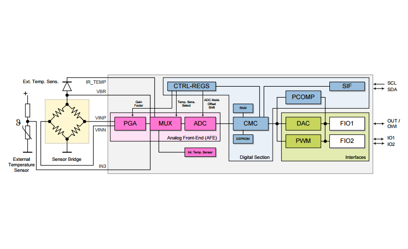
About Sensor Signal Conditioners
Most analog signals require some form of preparation before they can be digitized. Sensor signal conditioning is the manipulation of a sensor signal in a way that prepares it for the next stage of processing. Renesas' sensor signal conditioner ICs typically interface with two main sensor types: resistive bridges and differential capacitors. For each sensor type, further specialization allows selecting the optimal balance between price and performance for the required operating voltage and temperature range, gain, resolution, input/output format, and qualification level. Renesas' SSC ICs offer digital compensation of sensor offset, sensitivity, temperature drift, and nonlinearity in wide operational temperature ranges.
Advanced multi-market sensing platform ICs
-
Renesas Sensor Signal Conditioner ICs are all-in-one, energy-efficient products that are easy to use and are supported by advanced software and expert technical support staff with extensive sensor system design experience. A distinct advantage of our correction algorithms is that they are cali-brated and programmed in an efficient “single-pass” operation that lowers costs by reducing test time and loading of production test equipment without sacrificing precision. Renesas Sensor Signal Conditioner ICs also lower total system costs by simplifying sensor design with our excellent support tools, reducing external components, minimizing board space, and providing a faster migration to production.
Resistive Sensor Signal Conditioners (SSCs)
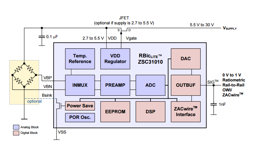
ZSC31010 Resistive Sensor Signal Conditioner with Analog Output
-
The ZSC31010 is a CMOS integrated circuit, which enables easy and precise calibration of resistive bridge sensors via EEPROM. When mated to a resistive bridge sensor, it will digitally calibrate offset and gain with the option to calibrate offset and gain coefficients and linearity over temperature. A second-order compensation can be enabled for temperature coefficients of gain or offset or bridge linearity. ZSC31010 communicates via Renesas ZACwire™ serial interface to the host computer and is easily mass calibrated in a Windows™ environment. Once calibrated, the output SIG™ pin can provide selectable 0 to 1 V absolute analog output; rail-to-rail ratiometric analog output; or digital serial output of bridge data with optional temperature data.
Features
- Digital compensation of sensor offset, sensitivity, temperature drift and non-linearity
- Accommodates differential sensor signal spans from 3 mV/V to 105 mV/V
- ZACwire™ one-wire interface (OWI)
- Internal temperature compensation and detection via bandgap PTAT(proportional to absolute temperature)
- Optional sequential output of both temperature and bridge readings on ZACwire™ digital output
- Output options: ratiometric analog voltage, absolute analog voltage, digital one-wire-interface
- Supply voltage 2.7V to 5.5 V, with external JFET 5.5V to 30 V
- Current consumption, depending on adjusted sample rate, 0.25 mA to 1 mA
- Wide operational range -50°C to +150°C
- Fast response time 1 ms
- High voltage protection up to 30V with external JFET
- Buffered and chopper-stabilized output DAC
Applications:
- Appliances / Filter Check, Refrigerant
- Consumer / Blood Pressure Meters, mobile phones, PDAs, wrist watches, Misc. Battery Applications
- Industrial / Process Control, Dataloggers
- Medical / Blood Pressure Meters, mobile phones, PDAs, wrist watches, Misc. Battery Applications
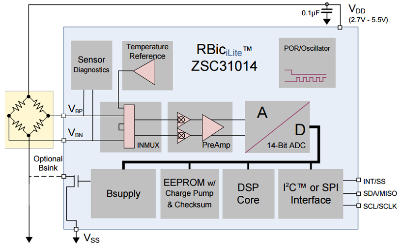
ZSC31014 Resistive Sensor Signal Conditioner with Digital Output
-
The ZSC31014 RBiciLite™ is a feature rich CMOS integrated circuit for high accuracy amplification and analog-to-digital conversion of a differential input signal. Perfect for low-cost applications, the ZSC31014 can perform offset, span, and 1st and 2nd order temperature compensation of the measured signal. Developed for correction of resistive bridge sensors, the ZSC31014can also provide a corrected temperature output through an internal or external sensor measurement. Digital compensation of signal offset, sensitivity, temperature and non-linearity is accomplished via an internal digital signal processor running a correction algorithm. Calibration coefficients are stored in a highly reliable non-volatile EEPROM. Measured and corrected bridge values provided at the digital output pins can easily be configured as I2C or SPI. Programming of the ZSC31014 is made simple by the I2C interface and the PC-controlled calibration software provided in the Renesas Evaluation Kit. Digital mating of the sensor with the signal conditioner is fast and precise, eliminating the overhead normally associated with trimming external components and multi-pass calibration routines.
Integrated diagnostics functions and low power stand-by-mode make theZSC31014 attractive for a variety of battery-operated applications, particularly products involving the use of a microcontroller for networking sensors.
Features
- Digital compensation of sensor offset, sensitivity, temperature drift and non-linearity
- Eight programmable analog gain and digital gain settings; accommodates bridges with spans < 1mV/V and high offset
- Internal or optional external temperature compensation for sensor correction and for corrected temperature out
- Diagnostic features (e.g., EEPROM signature, bridge connection checks, bridge short detection)
- 32-bit customer ID field for module traceability
- Digital single-pass calibration via I2C
- Fast power-up to data output response: 3ms
- Current consumption depends on programmed sample rate: as low as 200
Applications:
- Appliances / Filter Check, Refrigerant, Pressure Monitoring
- Automotive / Airflow, Differential Pressure, Process Control
- Consumer / Blood Pressure Meters, PDAs, Mobile Phones
- Industrial / Process Control, Dataloggers
- Medical / Blood Pressure Meters, PDAs, Mobile Phones
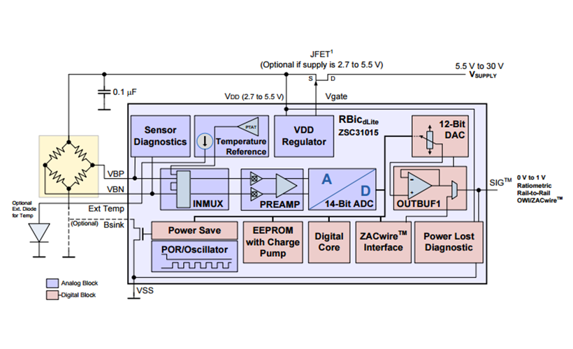
ZSC31015 Resistive Sensor Signal Conditioner with Analog Output and Diagnostic Features
-
The ZSC31015 (RBicdLite™) is a CMOS integrated circuit for highly accurate amplification and sensor-specific correction of bridge sensor signals. Digital compensation of sensor offset, sensitivity, temperature drift and non-linearity is accomplished via an internal digital signal processor running a correction algorithm with calibration coefficients stored in a non-volatile EEPROM. TheZSC31015 is adjustable to nearly all piezo-resistive bridge sensors. Measured and corrected bridge values are provided at the SIG™ pin, which can be configured as an analog voltage output or as a one-wire serial digital output. The digital one-wire interface can be used for a simple PC-controlled calibration procedure to program a set of calibration coefficients into an on-chipEEPROM. The calibrated ZSC31015 and a specific sensor are mated digitally: fast, precise, and without the cost overhead associated with trimming by external devices or laser. Integrated diagnostics functions make the ZSC31015particularly well suited for automotive applications.
Features
- Digital compensation of sensor offset, sensitivity, temperature drift and nonlinearity
- Programmable analog gain and digital gain; accommodates bridges with spans < 1mV/V and high offset
- Many diagnostic features on chip (e.g., EEPROM signature, bridge connection checks,bridge short detection, power loss detection)
- Independently programmable high and low clipping levels
- 24-bit customer ID field for module traceability
- Digital calibration and configuration via one-wire interface quick and precise
- Internal temperature compensation reference (no external components)
- Option for external temperature compensation with addition of single diode
- Output options: rail-to-rail ratiometric analog voltage (12-bit resolution), absolute analog voltage, digital one-wire-interface
- Supply voltage 2.7 to 5.5V, with external JFET, 5.5 to 30V
- Fast power-up to data output response, output available 5ms after power up
- Current consumption depends on programmed sample rate: 1mA down to 250
Capacitive SSCs
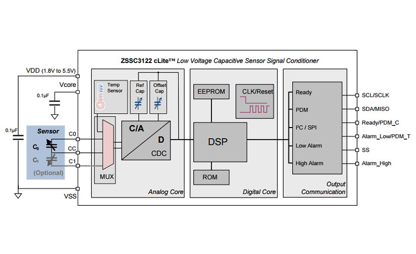
ZSSC3122 Low Voltage Capacitive Sensor Signal Conditioner with Digital Output
-
The ZSSC3122 cLite™ is a CMOS integrated circuit for accurate capacitance-to-digital conversion and sensor-specific correction of capacitive sensor signals. Digital compensation of sensor offset, sensitivity and temperature drift is accomplished via an internal digital signal processor running a correction algorithm with calibration coefficients stored in a non-volatile EEPROM. TheZSSC3122 is configurable for capacitive sensors with capacitances up to 10pF and a sensitivity of 125aF/LSB. It is compatible with both single capacitive sensors (both terminals must be accessible) and differential capacitive sensors. Measured and corrected sensor values can be output as I2C, SPI,PDM, or alarms. The I2C interface can be used for a simple PC-controlled calibration procedure to program a set of calibration coefficients into an on-chipEEPROM. The calibrated ZSSC3122 and a specific sensor are mated digitally: fast, precise, and without the cost overhead of trimming by external devices or laser.
Features
- Maximum target input capacitance: 10pF
- Sampling rates as fast as 0.7ms @ 8-bit, 1.6ms @ 10-bit, 5.0ms @ 12-bit, 18.5ms @ 14-bit
- Digital compensation of sensor: piece-wise 1st and 2nd order sensor compensation or up to 3rd order single-region sensor compensation
- Digital compensation of 1st and 2nd order temperature gain and offset drift
- Internal temperature compensation reference (no external components)
- Programmable capacitance span and offset
- Layout customized for die-die bonding with sensor for low-cost, high-density chip-on-board assembly
- Accuracy as high as ±0.25% full-scale output @ -20 to 125°C, 3V, 5V, Vsupply ±10% (see data sheet for restrictions)

ZSSC3123 Capacitive Sensor Signal Conditioner with Digital Output
-
The ZSSC3123 cLite™ is a CMOS integrated circuit for accurate capacitance-to-digital conversion and sensor-specific correction of capacitive sensor signals. Digital compensation of sensor offset, sensitivity and temperature drift is accomplished via an internal digital signal processor running a correction algorithm with calibration coefficients stored in a nonvolatile EEPROM. TheZSSC3123 is configurable for capacitive sensors with capacitances up to 260pF and a sensitivity of 125aF/LSB to 1pF/LSB depending on resolution, speed, and range settings. It is compatible with both single capacitive sensors (both terminals must be accessible) and differential capacitive sensors. Measured and corrected sensor values can be output as I2C, SPI, PDM, or alarms. The I2C interface can be used for a simple PC-controlled calibration procedure to program a set of calibration coefficients into an on-chip EEPROM. The calibrated ZSSC3123 and a specific sensor are mated digitally: fast, precise, and without the cost overhead of trimming by external devices or laser.
Features
- Maximum target input capacitance: 260pF
- Sampling rates as fast as 0.7ms @ 8-bit, 1.6ms @ 10-bit, 5.0ms @ 12-bit, 18.5ms @ 14-bit
- Digital compensation of sensor: piece-wise 1st and 2nd order sensor compensation or up to 3rd order single-region sensor compensation
- Digital compensation of 1st and 2nd order temperature gain and offset drift
- Internal temperature compensation reference (no external components)
- Programmable capacitance span and offset
- Layout customized for die-die bonding with sensor for low-cost, high-density chip-on-board assembly
- Accuracy as high as ±0.25% full-scale output @ -40°C to 125°C, 3V, 5V, Vsupply ±10% (see data sheet section 1.3 for restrictions)
Actuator and Motor Controller ICs
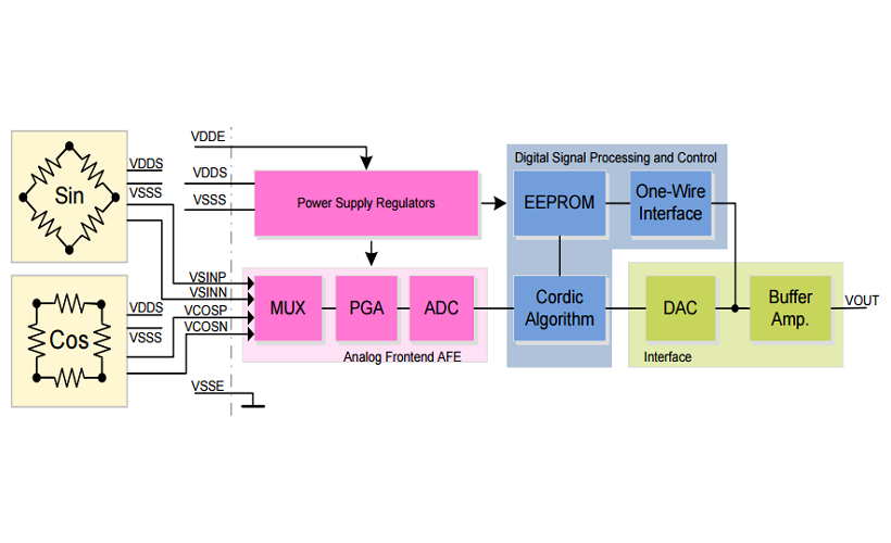
ZSSC5101 xMR Sensor Signal Conditionier
-
The ZSSC5101 is a CMOS integrated circuit for converting sine and cosine signals obtained from magnetoresistive bridge sensors into a ratiometric analog voltage with a user-programmable range of travel and clamping levels. The ZSSC5101 accepts sensor bridge arrangements for both rotational as well as linear movement. Depending on the type of sensor bridge, a full-scale travel range of up to 360 mechanical degrees can be obtained. Programming of the device is performed through the output pin, allowing in-line programming of fully assembled 3-wire sensors. Programming parameters are stored in an EEPROM and can be re-programmed multiple times. TheZSSC5101 is fully automotive-qualified with an ambient temperature range up to 150°C for SSOP-14 or 160°C for die.
Features
- Ratiometric analog output
- Up to 4608 analog steps
- Step size as small as 0.022°
- Programming through output pin via one-wire interface
- Offset and amplitude calibration of the bridge input signals
- Programmable linear transfer characteristic: zero position, angular range, upper and lower clamping levels, rising or falling slope
- Loss of magnet indication with programmable threshold level
- Accepts anisotropic, giant, and tunnel magnetoresistive bridge sensors (AMR, GMR and TMR)
- Programmable 32-bit user ID
- CRC, error detection, and error correction on EEPROM data
- Diagnostics: broken-wire detection
- Automotive-qualified to AEC-Q100, grade 0
ZAMC4100 Actuator and Motor Controller IC
-
The ZAMC4100 integrates an ARM® Cortex™-M0 microcontroller; eight power stages with integrated MOSFETs; SPI, UART and LIN2.1 communication interfaces; eight general-purpose digital input/output (I/O) pins; and four general-purpose analog inputs all in a single, compact 9x9mm QFN package. The ZAMC4100 addresses the growing demand for intelligent actuator/motor control in industrial, medical and automotive applications, and it is ideal for use where a small form factor is required or external components must be minimized.
Features
- Two main operation modes:
- NORMAL Mode with all functionality available
- SLEEP Mode with very low current consumption (less than 80
- Two main operation modes:
Resistive Automotive AEC-Q100-Qualified SSCs
- We enable IC solutions that reduce fuel consumption and CO2 emissions to help protect the environment. Our products include rugged AEC-Q100-certified ICs that expedite automotive product design by providing advanced sensor-signal conditioning and configurability while minimizing power consumption. Our sophisticated calibration and configuration techniques significantly reduce external component count and time to market for products that meet new emission-reduction standards.
ZSC31050 Advanced differential Sensor Signal Conditioner with Multiple output options
-
The ZSC31050 is a CMOS integrated circuit for amplification and sensor-specific correction of bridge sensor signals. The device provides digital compensation of sensor offset, sensitivity, temperature drift and non-linearity by a 16-bit RISC microcontroller running a correction algorithm. TheZSC31050 accommodates virtually any resistive bridge sensor (e.g., piezo-resistive and steel-membrane-based pressure sensors). In addition, the device can interface to a separate temperature sensor. The bi-directional digital interfaces (I2C, SPI, ZACwire™) can be used for a simple PC-controlled calibration procedure, encompassing writing and programming a set of calibration coefficients into an on-chip EEPROM. The ZSC31050 has been designed for industrial, medical and consumer applications and is specifically suited for most pressure sensors. It can also be used with force, torque, acceleration, angle, position and revolution sensors.
Features
- Digital compensation of sensor offset, sensitivity, temperature drift and non-linearity
- Accommodates nearly all bridge sensors via PGA and programmable ADC
- Capable of conditioning bridge sensor signals ranging from 1 to 275mV/V
- Sensor connections check and aging detection
- Temperature compensation via internal diode, external diode or bridge sensor element
- Output options: voltage (0 to 5V), current (4 to 20mA), PWM, I2C , SPI, ZACwire™ (one-wire interface), alarm
- Adjustable ADC resolution (up to 15-bit) versus sampling rate (up to 3.9kHz)
- Selectable bridge excitation: ratiometric voltage, constant voltage or constant current
- Input channel for separate temperature sensor
- Operation temperature range, depending on product version, up to -40°C to +150°C
- AEC-Q100 qualification (temperature grade 0)
- Supply voltage: +2.7V to +5.5V, with external JFET: 5 to 40 V
- Available in SSOP16 or as die
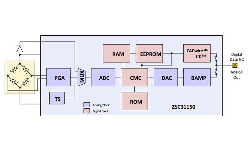
ZSC31150 Automotive Sensor Signal Conditioner
-
The ZSC31150 is a CMOS integrated circuit for amplification and sensor-specific correction of bridge sensor signals. The device provides digital compensation of sensor offset, sensitivity, temperature drift and non-linearity via a 16-bit RISC microcontroller running a correction algorithm. TheZSC31150 accommodates virtually any resistive bridge sensor (e.g., piezo-resistive and steel-membrane-based pressure sensors). The bi-directional digital interfaces (I2C and ZACwire™) can be used for a simple PC-controlled calibration procedure, encompassing writing and programming a set of calibration coefficients into an on-chip EEPROM. The ZSC31150 has been designed for automotive applications and is specifically suited for most pressure sensors. It can also be used with force, torque, acceleration, angle, position and revolution sensors. Safety applications (e.g. for braking or steering systems) are also supported by the ZSC31150's set of diagnostic functions. TheZSC31150 is optimized for automotive environments via protection circuitry and excellent electromagnetic compatibility.
Features
- Digital compensation of sensor offset, sensitivity, temperature drift and non-linearity
- Accommodates nearly all bridge sensors by PGA and programmable ADC
- Capable of conditioning bridge sensor signals ranging from 1 to 275mV/V
- Set of diagnostics functions needed for safety applications
- Temperature compensation via internal diode, external diode or bridge sensor element
- Output options: voltage (0 to 5V), I2C, ZACwire™ (one-wire interface)
- Adjustable ADC resolution (13 to 16 bits) versus sampling rate (up to 7.8kHz)
- High DAC resolution of 12-bit
- Selectable bridge excitation: ratiometric voltage or constant current
- Operation temperature range of (-40 to +125)°C or (-40 to +150)°C
- Supply voltage: 4.5V to +5.5V
- Available as DFN14, SSOP14, or die
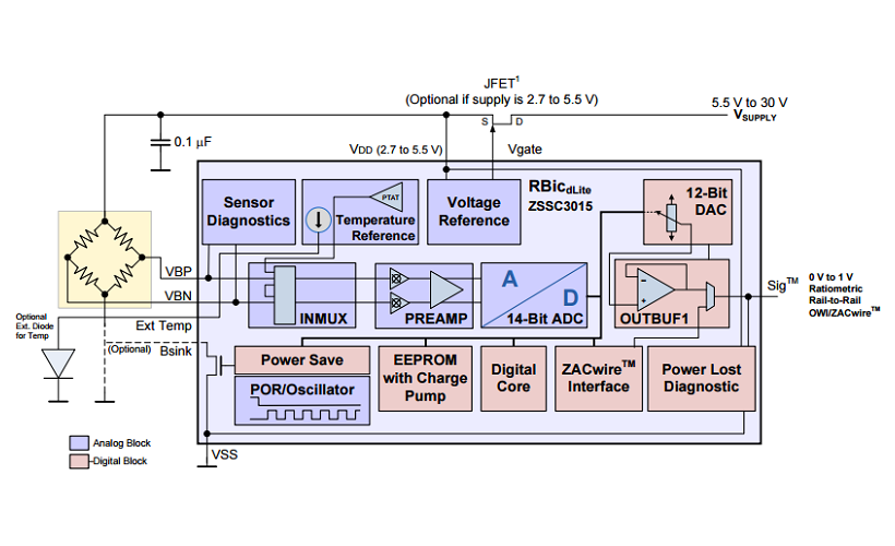
ZSSC3015 Resistive Sensor Signal Conditioner with Diagnostics- AEC Q 100 qualified
-
The ZSSC3015 RBicdLite-Auto™ sensor signal conditioner IC is adjustable to nearly all piezo-resistive bridge sensors. Measured and corrected bridge values are provided at the Sig™ pin, which can be configured as an analog voltage output or as a one-wire serial digital output. The ZACwire™ digital one-wire interface (OWI) can be used for a simple PC-controlled calibration procedure to program a set of calibration coefficients into an on-chipEEPROM. The calibrated ZSSC3015 and a specific sensor are mated digitally: fast, precise, and without the cost overhead associated with trimming by external devices or laser. Integrated diagnostics functions make theZSSC3015 particularly well-suited for automotive applications.
Features
- Digital compensation of sensor offset, sensitivity, temperature drift, and nonlinearity
- Programmable analog gain and digital gain; accommodates bridges with spans < 1mV/V and high offset
- Many diagnostic features on-chip (e.g., EEPROM signature, bridge connection checks, bridge short detection, power loss detection)
- Independently programmable high and low clipping levels
- 24-bit customer ID field for module traceability
- Internal temperature compensation reference (no external components)
- Option for external temperature compensation with addition of single diode
- Output options: rail-to-rail ratiometric analog voltage (12-bit resolution), absolute analog voltage, ZACwire™ digital one-wire interface
- Fast power-up to data out response, output available 5ms after power-up
- Current consumption depends on programmed sample rate and mode: 1mA down to 300μA (typ.)
- Fast response time: 1.4ms typical
- High voltage protection: ≤ 30V with external JFET
- AEC-Q100 qualified
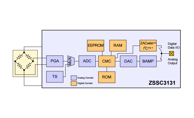
ZSSC3131 Sensor Signal Conditioner for Switch Applications
-
The ZSSC3131 is a member of the ZSSC313x product family of CMOSintegrated circuits designed for automotive and industrial sensor applications. All family members are well suited for highly accurate amplification and sensor-specific correction of resistive bridge sensor signals. An internal 16-bitRISC microcontroller running a correction algorithm compensates sensor offset, sensitivity, temperature drift, and non-linearity of the connected sensor element. The required calibration coefficients are stored by the single-pass calibration procedure in an on-chip EEPROM. The ZSSC3131 is optimized for simple switch and cost-sensitive sensor applications. The integrated adjustable digital filter offers the possibility to setup fast switching real-time applications as well as stabilized applications in the event of disturbed or unstable switching input signals.
Features
- Sample rate up to 200 Hz
- ADC resolution 13/14 bit
- Internal temperature compensation
- Integrated adjustable digital filter
- Digital compensation of sensor offset, sensitivity, temperature drift, and non-linearity
- Output options: Ratiometric analog voltage output (5% to 95% maximum, 12.4 bit resolution) or ZACwire™ (digital one-wire-interface)
- Sensor biasing by voltage
- High voltage protection up to 33 V
- Supply current: max. 5.5mA
- Reverse polarity and short circuit protection
- Operation temperature range as wide as -40°C to +150°C
- Traceability by user-defined EEPROM entries
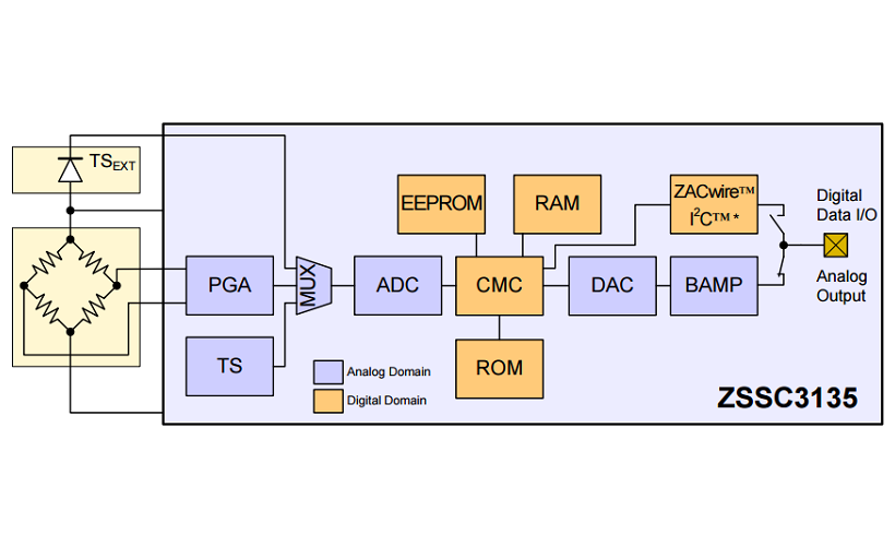
ZSSC3135 Fast Automotive SSC with Highly accurate amplification
-
The ZSSC3135 is a member of the ZSSC313x product family of CMOSintegrated circuits designed for automotive and industrial sensor applications. All family members are well suited for highly accurate amplification and sensor-specific correction of resistive bridge sensor signals. An internal 16-bitRISC microcontroller running a correction algorithm compensates sensor offset, sensitivity, temperature drift, and nonlinearity of the connected sensor element. The required calibration coefficients are stored by the single-pass calibration procedure in an on-chip EEPROM. The ZSSC3135 is specially designed for piezo-resistive bridge sensor elements. The amplification stage with an analog gain of 105 in combination with the optional temperature compensation using an external temperature sensor fits the requirements of piezo-resistive sensor applications perfectly.
Features
- Adjustable to nearly all resistive bridge sensor types, analog gain of 105, overall gain up to 420
- Sample rate up to 200 Hz
- ADC resolution 13/14 bit
- Safety functionality sensor connection
- External temperature sensor
- Digital compensation of sensor offset, sensitivity, temperature drift and nonlinearity
- Output options: ratiometric analog voltage output (5% to 95% maximum, 12.4 bit resolution) or ZACwire™ (digital one-wire-interface)
- Sensor biasing by voltage
- High voltage protection up to 33V
- Supply current: max. 5.5mA
- Reverse polarity and short circuit protection
- Operation temperature range as wide as -40°C to +150°C
- Traceability by user-defined EEPROM entries
ZSSC3154 Automotive Sensor Signal Conditioner with Dual analog output
-
The ZSSC3154 is an integrated circuit for highly accurate amplification and sensor-specific correction of a bridge sensor signal. Up to two temperature sensors can also be read in parallel. The circuitry provides different configurations of the analog outputs to show two measurement results simultaneously. This also allows generating a complementary bridge sensor signal, which is often required in safety-relevant applications. The ZSSC3154can take readings from two external temperature sensors to compensate the temperature drift of the bridge sensor signal and to output a separate temperature signal. An internal calibration microcontroller in addition with an on-chip EEPROM performs the digital compensation of the sensor offset, the sensitivity, the temperature drift, and the nonlinearity. The one-pass digital end-of-line calibration plus the integrated broken chip-detection supports automatic and highly efficient mass production.
Features
- Differential bridge sensor input
- Half-bridge sensor or temperature sensor input
- Digital compensation of offset, gain, nonlinearity and temperature dependency
- Two analog outputs, behavior programmable by EEPROM configuration
- Sequential analog output mode provides two measurands at one output pin
- Various on-chip diagnostic and safety features including sensor connection diagnostic and broken-chip detection
- 2 EEPROM words for arbitrary user data
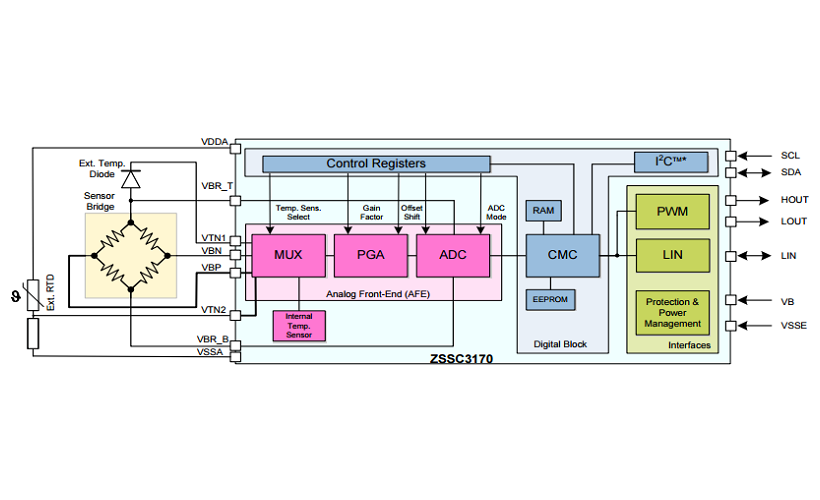
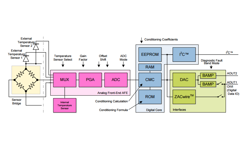
ZSSC3170 Automotive Sensor Signal Conditioner with LIN and PWM Interface
-
The ZSSC3170 is a CMOS integrated circuit for highly accurate amplification and sensor-specific correction of bridge sensor signals. Featuring a maximum analog gain of 420, as well as extended offset compensation capabilities, theZSSC3170 is adjustable to nearly all resistive bridge sensor types. Digital compensation of offset, sensitivity, temperature drift, and nonlinearity is accomplished via a 16-bit RISC microcontroller. Conditioning coefficients are stored in an EEPROM certified for automotive applications. Measured values are provided by one of the digital LIN or PWM interfaces. Each interface can support end-of-line calibration using the sensor output. Noise sensitivity is greatly reduced because the calibration equipment and the ZSSC3170 are mated digitally. For quick and easy evaluation and support for calibrating prototypes, IDT offers the ZSSC3170 SSC Evaluation Kit, which includes evaluation hardware, SSOP20 samples, and software.
Features
- Complies with LIN specifications 1.3 / 2.0 / 2.1
- Configurable LIN publisher frame content
- Data conversion rate of up to 430Hz fully utilizes the maximum LIN channel capacity of 20kbit/s
- PWM high-side and low-side switches, support for LIN communication for end-of-line calibration
- Digital compensation of offset, gain, temperature effects up to 2nd order, and nonlinearity up to 3rd order
- Compensation of temperature sensor offset, gain, and nonlinearity up to 2nd order.
- Internal or external temperature reference
- Media temperature sensing by diode or RTD
- Load-dump protection of the LIN pin up to ±40V
- Operating temperature range: -40°C to 125°C
- Extended operating temperature range: ≤150°C
- Accuracy: ±0.25% FSO @ -20°C to 85°C, ±0.50% FSO @ -40°C to 125°C, ±1.00% FSO @ -40°C to 150°C
- 3 EEPROM words available for optional use data
ZSSC416xKIT Evaluation Kit
-
The ZSSC416xKIT Evaluation Kit provides the hardware needed for configuration, calibration and evaluation of the ZSSC4161, ZSSC4162 andZSSC4165 Sensor Signal Conditioner (SSC) ICs. The user's PC can communicate with the ZSSC416x IC mounted on the ZSSC415x/6x/7x SSCEvaluation Board via the SSC Communication Board through a USBconnection. The Evaluation Kit Software is available on-line for free download.
The Evaluation Board can connect to the user's sensor or to the SSC Sensor Replacement Board (SRB). The SRB provides a replacement for an actual sensor and can be used for the first step of calibration or a dry-run calibration. On the SRB, the simulated resistive sensor signal is controlled by a potentiometer. The kit also includes three small populated test PCBs: each includes a ZSSC4161, ZSSC4162, or ZSSC4165 QFN sample and the required external components already mounted for facilitating user prototypes.For further information and support for the SSC Communication Board, visit the SSC-CB product page.
Boards can also be ordered separately. To enable product comparisons, this modular kit is compatible with other select IDT devices. Contact your local sales representative for more information.
Features
- ZSSC415x/6x/7x Evaluation Board with one sample mounted
- SSC Communication Board
- SSC Sensor Replacement Board
- USB Cable
- ZSSC4161_QFN_PCB
- ZSSC4162_QFN_PCB
- ZSSC4165_QFN_PCB
- 5 additional samples each of ZSSC4161, ZSSC4162 and ZSSC4165
- Vacuum suction pen
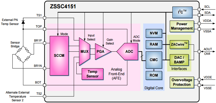
ZSSC4151 Automotive Sensor Signal Conditioner with Analog Output
-
The ZSSC4151 is a CMOS integrated circuit for highly accurate amplification and sensor-specific correction of resistive bridge sensor signals. Digital compensation of sensor offset, sensitivity, temperature drift, and non-linearity is accomplished via an internal 16-bit RISC microcontroller running a correction algorithm, with calibration coefficients stored in an integrated EEPROM. TheZSSC4151 is adjustable to nearly all resistive bridge sensor types. Measured values are provided at the analog voltage output and at the optional digital I2Cor the ZACwire™ interface, also referred to as the one-wire interface (OWI). The digital interfaces can be used for a simple PC-controlled calibration procedure to program a set of calibration coefficients into an on-chipEEPROM. The ZSSC4151 and the calibration equipment communicate digitally, so the noise sensitivity is greatly reduced. Digital calibration helps keep assembly cost low as no trimming by external devices or lasers is needed.
Features
- Safety and diagnostic functions that can enable support for automotive (ASIL B) and industrial (SIL 2) safety critical applications related to the ISO26262:2011 and IEC 61508 standards
- Digital compensation of sensor offset, sensitivity, temperature drift, and non-linearity
- Adjustable to nearly all full or half bridge sensors
- Analog gain of 200, supporting sensors with spans down to 1mV/V using the digital zooming option
- Output options: ratiometric 12-bit analog voltage output (e.g., 5-95% or 10-90%) with freely adjustable clamping or ZACwire™ digital one-wire-interface (OWI)
- Temperature compensation: internal or external diode, bridge external series resistance, or RTD
- Sensor biasing by internal voltage
- High voltage and reverse polarity protection up to 40V at all module pins:VDDE, VSSE, and AOUT
- Maximum supply current: 7mA
- Short-circuit protection for AOUT
- Traceability via user-defined registers
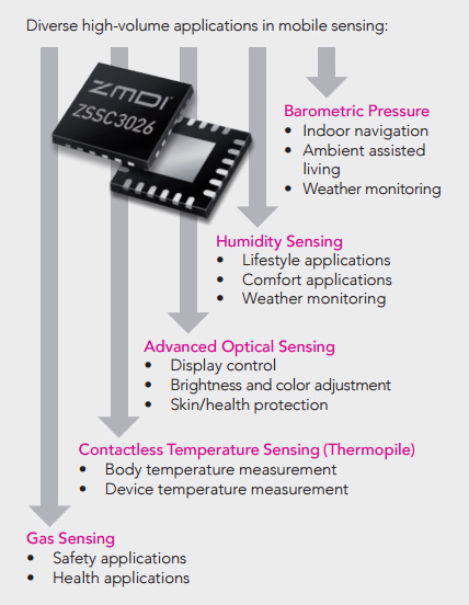
Mobile sensing
-
Industry leaders are predicting double-digit growth for the global market for mobile sensors, which is expected to expand to over 22 billion dollars by 2018. Renesas’s next-generation sensing technology can shorten critical time-to-market essential to meeting the increasing demands for smaller mobile products with more sophisticated features.
With new solutions rapidly emerging in the market for mobile sensing systems and higher levels of integration driving new development, ZMDI is well placed to offer solutions that advance opportunities in this high-growth market. With highly integrated products providing advanced signal conditioning and sensing capabilities, Renesas is positioned to be a true partner to tier-one suppliers, emerging market suppliers, MEMS suppliers, and reference design houses. For example, our ZOPT3100 includes an ambient light sensor (ALS), a color sensor (CS), a proximity sensor (PS), and an integrated IR LED driver on a single chip.
Our energy-efficient, battery-optimized sensor signal conditioners (SSCs) enable diverse mobile applications, with current consumption as low as 930μA in operating mode or 20nA in sleep mode. Renesas mobile SSC ICs offer digital compensation of sensor offset, sensitivity, temperature drift, and non-linearity in operational temperature ranges as wide as -40°C to +125°C.
Enables inteligent sensors
Technology
-
Innovative environmental mobile sensing solutions based on advanced sensor technologies
• Resistive bridge sensors
• Capacitive sensors
• Thermopile sensors
• Light sensors
Sensors
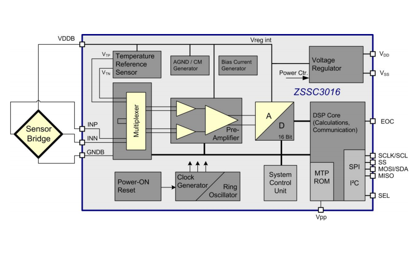
ZSSC3016
-
The ZSSC3016 is a sensor signal conditioner (SSC) integrated circuit for high-accuracy amplification and analog-to-digital conversion of a differential input signal. Designed for high resolution altimeter module applications, theZSSC3016 can perform offset, span, and 1st and 2nd order temperature compensation of the measured signal. Developed for correction of resistive bridge sensors, it can also provide a corrected temperature output measured with an internal sensor. The measured and corrected bridge values are provided at the digital output pins, which can be configured as I2C (≤ 3.4MHz) or SPI (≤ 20MHz). Digital compensation of signal offset, sensitivity, temperature, and non-linearity is accomplished via an 18-bit internal digital signal processor (DSP) running a correction algorithm. Calibration coefficients are stored on-chip in a highly reliable, nonvolatile, multiple-time programmable (MTP) memory. Programming the ZSSC3016 is simple via the serial interface and the PC-controlled calibration software provided in the Renesas Evaluation Kit. The interface is used for the PC-controlled calibration procedure, which programs the set of calibration coefficients in memory. Digital mating of the sensor with the signal conditioner is fast and precise, eliminating the overhead normally associated with trimming external components and multi-pass calibration routines.
Features
- Flexible, programmable analog front-end design, up to 16-bit scalable, charge-balancing two-segment analog-to-digital converter (ADC)
- Fully programmable gain amplifier accepting sensors from 14 to 72 (linear factor)
- Internal auto-compensated temperature sensor
- Digital compensation of individual sensor offset
- 1st and 2nd order digital compensation of sensor gain
- Digital compensation of 1st and 2nd order temperature gain and offset drift
- Intelligent power management unit
- Layout customized for die-die bonding with sensor for high-density chip-on-board assembly
- Typical sensor elements can achieve accuracy of better than ±0.10% FSO @ -40 to 85 °C
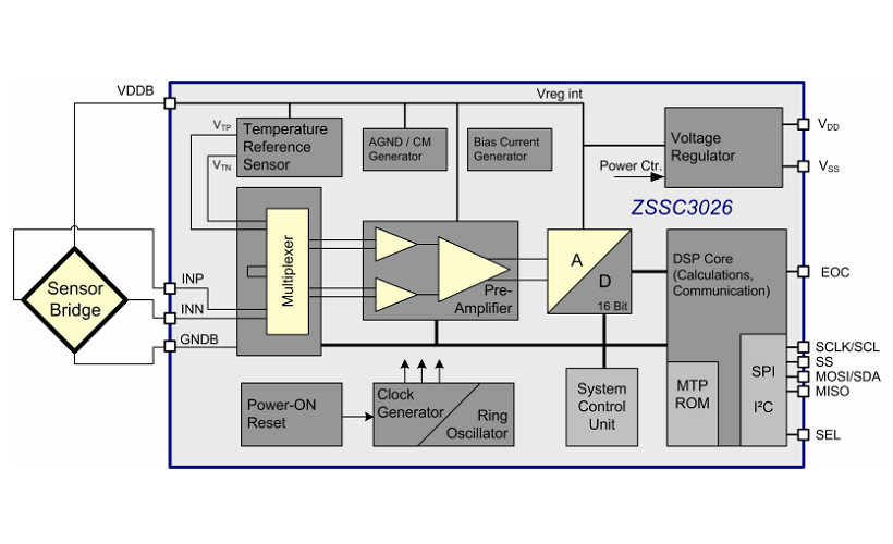
ZSSC3026
-
The ZSSC3026 is a sensor signal conditioner (SSC) integrated circuit for high-accuracy amplification and analog-to-digital conversion of a differential input signal. Designed for high-resolution altimeter module applications, theZSSC3026 can perform offset, span, and 1st and 2nd order temperature compensation of the measured signal. Developed for correction of resistive bridge sensors, it can also provide a corrected temperature output measured with an internal sensor. The measured and corrected bridge values are provided at the digital output pins, which can be configured as I2C (≤ 3.4MHz) or SPI (≤ 20MHz). Digital compensation of signal offset, sensitivity, temperature, and non-linearity is accomplished via an 18-bit internal digital signal processor (DSP) running a correction algorithm. Calibration coefficients are stored on-chip in a highly reliable, non-volatile, multiple-time programmable (MTP) memory. Programming the ZSSC3026 is simple via the serial interface. The IC-internal charge pump provides the MTP programming voltage. The interface is used for the PC-controlled calibration procedure, which programs the set of calibration coefficients in memory. Digital mating of the sensor with the signal conditioner is fast and precise, eliminating the overhead normally associated with trimming external components and multi-pass calibration routines.
Features
- Flexible, programmable analog front-end design, up to 16-bit scalable, charge-balancing two-segment analog-to-digital converter (ADC)
- Fully programmable gain amplifier accepting sensors from 14 to 72 (linear factor)
- Internal auto-compensated temperature sensor
- Digital compensation of individual sensor offset
- 1st and 2nd order digital compensation of sensor gain
- Digital compensation of 1st and 2nd order temperature gain and offset drift
- Intelligent power management unit
- Layout customized for die-die bonding with sensor for high-density chip-on-board assembly
- Typical sensor elements can achieve accuracy of less than ±0.10% FSO @ -40 to 110 °C
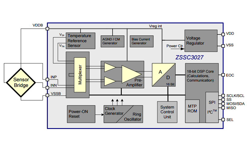
ZSSC3027
-
The ZSSC3027 is a sensor signal conditioner (SSC) integrated circuit for high-accuracy amplification and analog-to-digital conversion of a differential input signal. Designed for high-resolution altimeter module applications, theZSSC3027 can perform offset, span, and 1st and 2nd order temperature compensation of the measured signal. Developed for correction of resistive bridge sensors, it can also provide a corrected temperature output measured with an internal sensor. The measured and corrected bridge values are provided at the digital output pins, which can be configured as either I2C (≤ 3.4MHz) or SPI (≤ 20MHz). Digital compensation of signal offset, sensitivity, temperature, and non-linearity is accomplished via an 18-bit internal digital signal processor (DSP) running a correction algorithm. Calibration coefficients are stored on-chip in a highly reliable, non-volatile, multiple-time programmable (MTP) memory. Programming the ZSSC3027 is simple via the serial interface. The IC-internal charge pump provides the MTP programming voltage. The interface is used for the PC-controlled calibration procedure, which programs the set of calibration coefficients in memory. The ZSSC3027 provides accelerated signal processing in order to support high-speed control, safety, and real-time sensing applications. It complements Renesas ZSSC30x6 products.
Features
- Flexible, programmable analog front-end design, up to 16-bit scalable, charge-balancing two-segment analog-to-digital converter (ADC)
- Fully programmable gain amplifier accepting sensors from 14 to 72 (linear factor)
- Internal auto-compensated temperature sensor
- Digital compensation of individual sensor offset
- 1st and 2nd order digital compensation of sensor gain as well as of 1st and 2nd order temperature gain and offset drift
- Layout optimized for stacked-die bonding for high-density chip-on-board assembly
- Typical sensor elements can achieve accuracy of better than ±0.10% full-scale output @ -40°C to 85°C
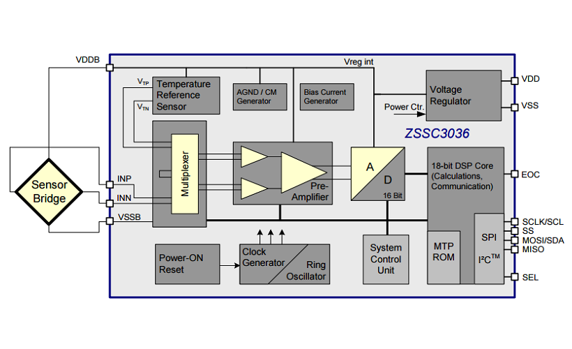
ZSSC3036
-
The ZSSC3036 is a sensor signal conditioner (SSC) integrated circuit for high-accuracy amplification and analog-to-digital conversion of a differential input signal. Designed for high-resolution altimeter module applications, theZSSC3036 can perform offset, span, and 1st and 2nd order temperature compensation of the measured signal. Developed for correction of resistive bridge sensors, it can also provide a corrected temperature output measured with an internal sensor. The measured and corrected bridge values are provided at the digital output pins, which can be configured as I2C (≤ 3.4MHz) or SPI (≤ 20MHz). Digital compensation of signal offset, sensitivity, temperature, and non-linearity is accomplished via an 18-bit internal digital signal processor (DSP) run
Features
- Flexible, programmable analog front-end design, up to 16-bit scalable, charge-balancing two-segment analog-to-digital converter (ADC)
- Fully programmable gain amplifier accepting sensors from 14 to 72 (linear factor)
- Internal auto-compensated temperature sensor
- Digital compensation of individual sensor offset
- 1st and 2nd order digital compensation of sensor gain as well as of 1st and 2nd order temperature gain and offset drift
- Fast sensing: 16-bit conditioned sensor signal measurement rate at more than 200s-1
- Typical sensor elements can achieve accuracy of better than ±0.10% full-scale output at -40 to 110°C
ZSSC3218
-
The ZSSC3218 is a sensor signal conditioner (SSC) integrated circuit for high-accuracy amplification and analog-to-digital conversion of a differential or pseudo-differential input signal. Designed for high-resolution sensor module applications, the ZSSC3218 can perform offset, span, and 1st and 2nd order temperature compensation of the measured signal. Developed for correction of resistive bridge or absolute voltage sensors, it can also provide a corrected temperature output measured with an internal sensor. The measured and corrected sensor values are provided at the digital output pins, which can be configured as I2C (≤ 3.4MHz) or SPI (≤ 20MHz). Digital compensation of signal offset, sensitivity, temperature, and non-linearity is accomplished via a 26-bit internal digital signal processor (DSP) running a correction algorithm. Calibration coefficients are stored on-chip in a highly reliable, nonvolatile, multiple-time programmable (MTP) memory. Programming the ZSSC3218 is simple via the serial interface. The interface is used for the PC-controlled calibration procedure, which programs the set of calibration coefficients in memory. The ZSSC3218 provides accelerated signal processing, increased resolution, and improved noise immunity in order to support high-speed control, safety, and real-time sensing applications with the highest requirements for energy efficiency.
Features
- Flexible, programmable analog front-end design, up to 18-bit analog-to-digital converter (ADC)
- Fully programmable gain amplifier for optimizing sensor signals: gain range 6.6 to 216 (linear)
- Internal auto-compensated temperature sensor
- Digital compensation of individual sensor offset, 1st and 2nd order digital compensation of sensor gain as well as 1st and 2nd order temperature gain and offset drift
- Programmable interrupt operation
- High-speed sensing, e.g. 16-bit conditioned sensor signal measurement rate >500s-1
- Typical sensor elements can achieve an accuracy of better than ±0.10% full-scale output at -40°C to 85°C
Battery Management
-
Battery Sensor ICs
Renesas battery sensor ICs accurately determine the charge condition of the battery based on inputs including charge and discharge currents, battery voltage, temperature, and aging. Both voltage and current are measured with two highly linear, synchronous 24-bit analog-to-digital converters.
Battery Charge Measurement in Automotive Applications
Measuring charge and discharge currents is particularly challenging as the battery monitoring IC must be capable of precisely measuring milliampere currents when the engine is turned off and up to more than one thousand amperes when the engine is started.Renesas battery sensor ICs can achieve this requirement by means of a shunt-resistor-based current measurement technique combined with a highly dynamic embedded programmable gain amplifier.

ZSSC1750: Data Acquisition System Basis Chip with Dual-Channel ADC
-
The ZSSC1750 is a System Basis Chip (SBC) with a dual-channel ADC for battery sensing/management in automotive, industrial, and medical systems. The ZSSC1750 features an SPI interface. One of the two input channels measures the battery current IBAT via the voltage drop at the external shunt resistor. The second channel measures the battery voltage VBAT and the temperature. By simultaneously measuring VBAT and IBAT, it is possible to determine dynamically the internal resistance of the battery, Rdi, which is correlated with the state-of-health (SOH) of the battery. By integrating IBAT, it is possible to determine the state-of-charge (SOC) and the state-of-function (SOF) of the battery. During Sleep Mode, the system makes periodic measurements to monitor the discharge of the battery. Measurement cycles are controlled by user software and include various wake-up conditions. TheZSSC1750 is optimized for ultra-low power consumption drawing only 60μA or less in this mode.
Features
- Two high-precision 24-bit sigma-delta ADCs (18-bit with no missing codes)
- Sample rate: 1Hz to 16kHz
- On-chip voltage reference (5ppm/K typical)
- Current channel IBAT offset error: ≤ 10mA
- Current channel IBAT resolution: ≤ 1mA
- Current channel programmable gain: 4 to 512
- Current channel maximum differential input stage input range: ±300mV
- Voltage channel input range: 4 to 28.8V
- Voltage channel accuracy: ±60ppm full-scale range = 1.73mV
- Temperature channel external temperature sensor (NTC)
- Temperature channel factory-calibrated internal temp. sensor: ±2°C
- LIN 2.1/SAE J2602-1 transceiver
- Normal Mode typical current consumption: 12mA
- Sleep Mode typical current consumption: ≤ 60μA
ZSSC1751: Data Acquisition System Basis Chip with Dual-Channel ADC
-
The ZSSC1751 is a System Basis Chip (SBC) with a dual-channel ADC for battery sensing/management in automotive, industrial, and medical systems. The ZSSC1751 features an SPI interface and an integrated LIN 2.1 transceiver. One of the two input channels measures the battery current IBATvia the voltage drop at the external shunt resistor. The second channel measures the battery voltage VBAT and the temperature. By simultaneously measuring VBAT and IBAT, it is possible to determine dynamically the internal resistance of the battery, Rdi, which is correlated with the state-of-health (SOH) of the battery. By integrating IBAT, it is possible to determine the state-of-charge (SOC) and the state-of-function (SOF) of the battery. During Sleep Mode, the system makes periodic measurements to monitor the discharge of the battery. Measurement cycles are controlled by user software and include various wake-up conditions. The ZSSC1751 is optimized for ultra-low power consumption drawing only 60μA or less in this mode.
The related product ZSSC1750 offers the same functionality with an additionalLIN interface feature.Features
- Two high-precision 24-bit sigma-delta ADCs (18-bit with no missing codes)
- Sample rate: 1Hz to 16kHz
- On-chip voltage reference (5ppm/K typical)
- Current channel IBAT offset error: ≤ 10mA
- Current channel IBAT resolution: ≤ 1mA
- Current channel programmable gain: 4 to 512
- Current channel maximum differential input stage input range: ±300mV
- Voltage channel input range: 4 to 28.8V
- Voltage channel accuracy: ±60ppm full-scale range = 1.73mV
- Temperature channel external temperature sensor (NTC)
- Temperature channel factory-calibrated internal temp. sensor: ±2°C
- Normal Mode typical current consumption: 12mA
- Sleep Mode typical current consumption: ≤ 60μA
ZSSC1956 Intelligent Battery Sensor IC
-
The ZSSC1956 is a dual-channel ADC with an embedded microcontroller for battery sensing/management in automotive, industrial, and medical systems. One of the two input channels measures the battery current IBAT via the voltage drop at the external shunt resistor. The second input channel measures the battery voltage VBAT and the temperature. An integrated flash memory is provided for customer-specific software; e.g., dedicated algorithms for calculating the battery state. During Sleep Mode (e.g., engine is off), the system makes periodic measurements to monitor the discharge of the battery. Measurement cycles are controlled by the software and include various wake-up conditions. The ZSSC1956 is optimized for ultra-low power consumption and draws only 100
Features
- High-precision 24-bit sigma-delta ADC (18-bit with no missing codes)
- Sample rate: 1Hz – 16kHz
- On-chip voltage reference (5ppm/K typical)
- Current channel IBAT offset error: ≤10mA
- Current channel IBAT resolution: ≤1mA
- Current channel programmable gain: 4 to 512
- Current channel differential input stage input range: ± 300mV
- Voltage channel input range: 4 to 28.8V
- Voltage channel accuracy: better than ±2mV
- Temperature channel internal temperature sensor: ± 2°C
- Temperature channel external temperature sensor (NTC)
- On-chip precision oscillator (1%) and on-chip low-power oscillator
- ARM® Cortex™-M0 microcontroller: 32-bit core, 10MHz to 20MHz
- 96kB Flash/EE Memory with ECC, 8kB SRAM
- LIN2.2 /SAE J2602-2 compliant
- Directly connected to 12V battery supply
- Normal Mode current consumption: 10mA to 20mA
- Low-Power Mode current consumption: ≤ 100µA
ZSPM4121: Under-Voltage Load Switch for Smart Battery Management
-
The ZSPM4121 battery management load switch can be used to protect a battery from excessive discharge. It actively switches the battery power source off if it drops to a set threshold (Off Mode). When the input battery voltage is above the threshold, the load switch is on (On Mode). The ZSPM4121threshold voltage (VTHRESH) is programmed at manufacturing to a set point in the range of 1.2V to 4.2V with 100mV steps between options. When the input battery voltage has been switched off by the ZSPM4121, the quiescent current draw on the battery is in the order of 100pA (typical). The quiescent current in the on state is as low as 70nA. The ZSPM4121 consists of an internally generated threshold voltage, a comparator with hysteresis, slew rate control for the load switch, a P-channel load switch, and an open-drain indicator pin. The 500mV hysteresis between the Off Mode and the On Mode prevents intermittent operation. The ZSPM4121 also provides over-current protection.
Features
- Power source is actively switched off when VCC drops below a set threshold (programmed at manufacturing)
- Wide input voltage range: 1.2V to 5.5V
- Threshold voltage options: 1.2V to 4.2V in 100mV steps (factory programmed)
- Supervisory over-current limit shutdown
- Low drop-out disconnect from VCC to loads
- Controlled turn-on slew rate
- 500mV Off Mode to On Mode hysteresis
- Over-current shutdown (3A)
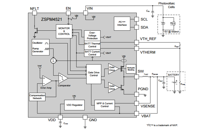
ZSPM4521: 1.5A Solar Charger Li-ION
-
The ZSPM4521 is a DC/DC synchronous switching lithium-ion (Li-Ion) battery charger with fully integrated power switches, internal compensation, and full fault protection. It uses a temperature-independent photovoltaic maximum power point tracking (MPPT) function to optimize power output from the source during Full-Charge Constant-Current (CC) Mode. Its switching frequency of 1MHz enables the use of small filter components, resulting in smaller board space and reduced bill-of material costs. During Full-Charge Constant-Current Mode, the duty cycle is controlled by the MPPT regulator. Once the battery’s termination voltage is reached, the regulator operates in Constant Voltage Mode. In this mode, the ZSPM4521 modulates the charging current until the battery reaches full charge. When the regulator is disabled (the EN pin is low), the device draws 10µA (typical) quiescent current (Disabled Mode). TheZSPM4521 includes supervisory reporting through the NFLT (inverted fault) open-drain output to interface other components in the system. Device programming is achieved by an I²C interface through the SCL and SDA pins.
Features
- Temperature-independent photovoltaic maximum power tracking (MPPT) regulator
- VBAT reverse-current blocking
- Programmable temperature-compensated termination voltage: 3.94V to 4.18V ± 1%
- User-programmable maximum charge current: 50mA to 1500mA
- Supervisor for VBAT reported at the NFLT pin
- Input supply under-voltage lockout
- Full protection for VBAT over-current, over-temperature, VBAT over-voltage, and charging timeout
- Charge status indication
- I2C program interface with EEPROM registers
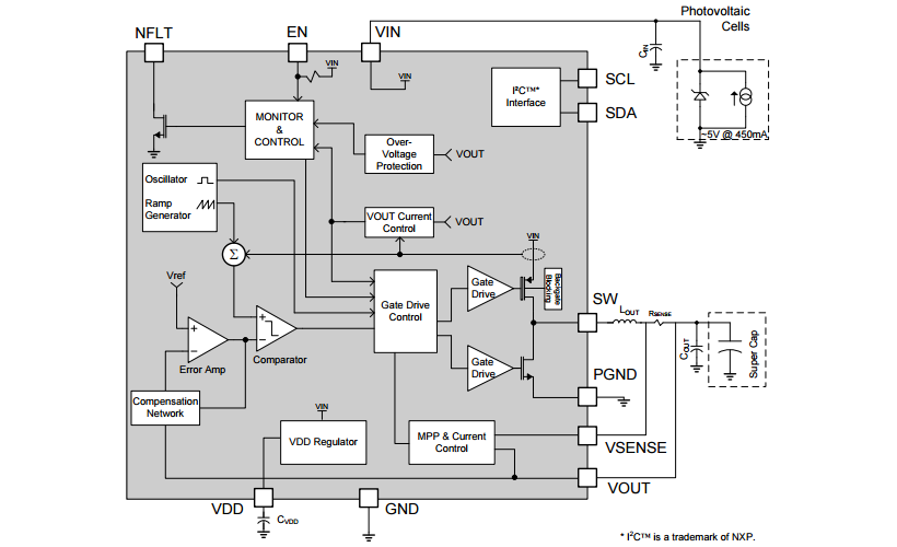
ZSPM4523: 1.5A Solar Charger Regulator for Super Capacitors
-
The ZSPM4523 is a DC/DC synchronous switching super capacitor charger with fully integrated power switches, internal compensation, and full fault protection. It uses a temperature-independent photovoltaic maximum power point tracking (MPPT) calculator to optimize power output from the source during Full-Charge Mode. Its 1MHz switching frequency allows using small filter components, which results in smaller board space and reduced bill-of-material costs. In Full-Charge Mode, the duty cycle is controlled by the MPPTfunction. Once the termination voltage is reached, the regulator operates in Constant Voltage Mode. When the regulator is disabled (the EN pin is low), the device draws 10µA (typical) quiescent current from VOUT. The ZSPM4523integrates a wide range of protection circuitry, including input supply under-voltage lockout, output over-voltage protection, current limiting, and thermal shutdown. The ZSPM4523 includes supervisory reporting via the NFLT (Inverted Fault) open-drain output to interface other components in the system. Device programming is achieved by the I²C interface through the SCL and SDA pins.
Features
- Temperature-independent MPPT regulation
- VOUT reverse-current blocking
- Programmable temperature-compensated termination voltage: 2.48 to 2.74 V ± 1%
- User programmable maximum charge current: 50mA to 1500mA
- Input supply under-voltage lockout
- Full protection for VOUT over-voltage
- I2C program interface with EEPROM registers
- Charge status indication
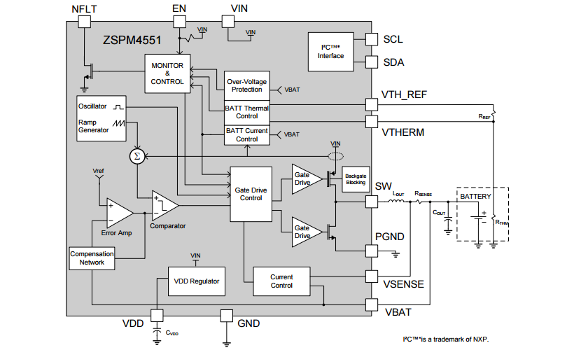
ZSPM4551: 1.5A Charger Li-ION
-
The ZSPM4551 is a DC/DC synchronous switching lithium-ion (Li-Ion) battery charger with fully integrated power switches, internal compensation, and full fault protection. Its switching frequency of 1MHz enables the use of small filter components, resulting in smaller board space and reduced BOM cost.
In Full-Charge Constant-Current Mode, the regulation is for constant current (CC). Once termination voltage is reached, the regulator operates in voltage mode. When the regulator is disabled (the EN pin is low), the device draws 10µA (typical) quiescent current.
The ZSPM4551 includes supervisory reporting through the NFLT (inverted fault) open-drain output to interface other components in the system. Device programming is achieved by an I²C™ interface through the SCL and SDA pins. (Note: I2C™ is a trademark of NXP.).
Smart Power Management Solutions
-
Designers of today’s high performance systems face many challenges: competitive features, regulatory requirements, solution stability, aggressive time-tomarket, and quick migration to manufacturing. Often the power requirements of the system are not well understood in the early part of the design process and features that help improve overall system reliability are becoming key differentiators. Consequently power system designers need solutions that are high performance, easily optimized, fully-featured, easy to use, flexible, and reusable.
Renesas smart power management chipsets provide designers with a complete range of high efficiency solutions to meet low, medium, and high power requirements. Configurability via hardware or software ensures optimum flexibility and reusability of your design. Our solutions offer optional communications for telemetry and fault reporting allowing easier implementation in smart managed systems to meet system reliability, energy efficiency, and regulatory requirements.
Renesas digital smart power management ICs are supported by our easy-to-use PC-based Pink Power Designer™ design optimizer tool. A key advantage of this software and our true digital architecture is the ability to make real time trade-offs between performance, size, and cost. The software helps maintain your design investment as the resulting solution can be easily migrated to meet different power requirements.
Typical Applications:
- Telecommunications equipment and base stations
- Network router and switches
- FPGAs
- Industrial and high-end PCs
- Server and storage units
- Wireless access points, cable modems
- Set-top boxes
Single-Phase Power Family
ZSPM1000 True Digital PWM Controller (Single-Phase, Single-Rail)
- The ZSPM1000 is a configurable true-digital single-phase PWM controller for high-current, non-isolated DC/DC supplies. It operates as a synchronous step-down converter in a single-rail and single-phase configuration. TheZSPM1000 integrates a digital control loop, optimized for maximum flexibility and stability, as well as load step and steady-state performance. In addition, a rich set of protection and monitoring functions is provided. On-chip, non-volatile memory (NVM) and an I2C interface facilitate configuration.Renesas PC-based Pink Power Designer™ provides a user-friendly and easy-to-use interface to the device for communication and configuration. It can guide the user through the design of the digital compensator and offers intuitive configuration methods for additional features, such as protection and sequencing.
Features
- Programmable digital control loop
- Advanced, digital control techniques: Tru-sample Technology™, State-Law Control™ (SLC), and Sub-cycle Response™ (SCR)
- Improved transient response and noise immunity
- Discontinuous conduction mode (DCM)
- Protection features: over-current protection, over-voltage protection (VIN,VOUT), under-voltage protection (VIN, VOUT), overloaded startup, and restart and delay
- Fuse-based NVM for improved reliability
- Operation from a single 5V or 3.3V supply
- Optional PMBus™ address selection without external resistors
ZSPM2000: True Digital PWM Controller with Integrated MOSFET Driver
-
The ZSPM2000 is a configurable true-digital single-phase PWM controller for high-current, non-isolated DC/DC supplies. The ZSPM2000 includes a high-speed MOSFET driver for a synchronous step-down converter in a single-rail and single-phase configuration. The ZSPM2000 integrates a digital control loop, optimized for maximum flexibility and stability, as well as load step and steady-state performance. In addition, a rich set of protection and monitoring functions is provided. On-chip, non-volatile memory (NVM) and an I²C interface facilitate configuration.Renesas PC-based Pink Power Designer™ graphical user interface (GUI) provides a user-friendly and easy-to-use interface to the device for communication and configuration. It can guide the user through the design of the digital compensator and offers intuitive configuration methods for additional features, such as protection and sequencing.
Features
- Programmable digital control loop
- Advanced digital control techniques: Tru-sample Technology™, State-Law Control™ (SLC), and Sub-cycle Response™ (SCR)
- Improved transient response and noise immunity
- Protection features: over-current protection, over-voltage protection (VIN,VOUT), under-voltage protection (VIN, VOUT), overloaded startup, and restart and delay
- Integrated MOSFET driver with adaptive anti-cross-conduction protection
- Fuse-based NVM for improved reliability
- Operation from a single 5V or 3.3V supply
- Optional PMBus™ address selection without external resistors
ZSPM1025A True Digital PWM Controller (Single-Phase, Single-Rail)
-
IDT's ZSPM1025A single-phase digital PWM controller is optimally configured for use with the Murata Power Solutions 25A Power Block OKLP-X/25 and provides a quick route to proven, high-performance smart digital power solutions. The ZSPM1025A PWM controller integrates a digital control loop optimized for ultra-fast transient response, steady-state performance, stability and design flexibility. For improved system reliability, a rich set of protection and monitoring functions is provided. The ZSPM1025A features user-selectable, preconfigured compensators in the digital control loop optimized for use with the Murata Power Solutions 25A power block.Renesas easy-to-use Pink Power Designer™ software enables solutions that have fully customizable output voltage and output capacitance. PMBus™ digital communications is available for monitoring, configurable protection and sequencing. A downloadable reference solution is available, including a graphical user interface, layout guidelines, bill of materials and step-by-step instructions. It is ready to be immediately implemented in the application design.
Features
- Programmable application-optimized digital control loop
- Advanced, digital control techniques: Tru-sample Technology™, State-Law Control™ (SLC), and Sub-cycle Response™ (SCR)
- Improved transient response and noise immunity
- Protection features: over-current protection, over-voltage protection (VIN,VOUT), under-voltage protection (VIN, VOUT), overloaded startup, over-temperature protection (internal, external), and continuous retry (“hiccup”) mode for fault conditions
- Optimized pre-configured digital loop compensators for the Murata Power Block
- PMBus™ configuration for output voltage and monitoring
- Operation from a single 5V or 3.3V supply
Analog DC-DC Regulator Family
Step-down (Buck) Regulators
-
Renesas energy-efficient, synchronous step-down regulators for non-isolated applications provide up to 95% efficiency. The step-down regulators feature integrated driver and power FETs, capable of leveraging a wide input voltage range and supporting up to 12A of output current.
About Step-down Switching Regulators
A step-down, or buck, switching regulator takes an input voltage and efficiently converts it into a regulated lower voltage. Devices typically come with fixed or adjustable output voltages. A good buck regulator will provide high-efficiency and excellent transient response under all load conditions. Buck regulators will often provide special features to ensure protection of the IC during fault conditions, such as under-voltage lockout, thermal shutdown, soft-start, currently limiting, and short-circuit protection.