FormFactor

Videos
Loading the player ...
- Offer Profile
- FormFactor, Inc. is a leading provider of essential test and measurement technologies along the full IC life cycle – from characterization, modeling, reliability, and design de-bug, to qualification and production test.
Semiconductor companies rely upon our products and services to accelerate profitability by optimizing device performance and advancing yield knowledge.
Through education, collaboration and innovation, FormFactor helps customers navigate the technology transitions essential to next-generation applications. Markets like data center, mobile and automotive are growing rapidly, and our experts are helping test engineers drive precision into volume. By expanding its broad-based test expertise across the design-to-silicon continuum, FormFactor can provide a comprehensive perspective, to become a trusted partner in the semiconductor industry ecosystem.
Product Portfolio
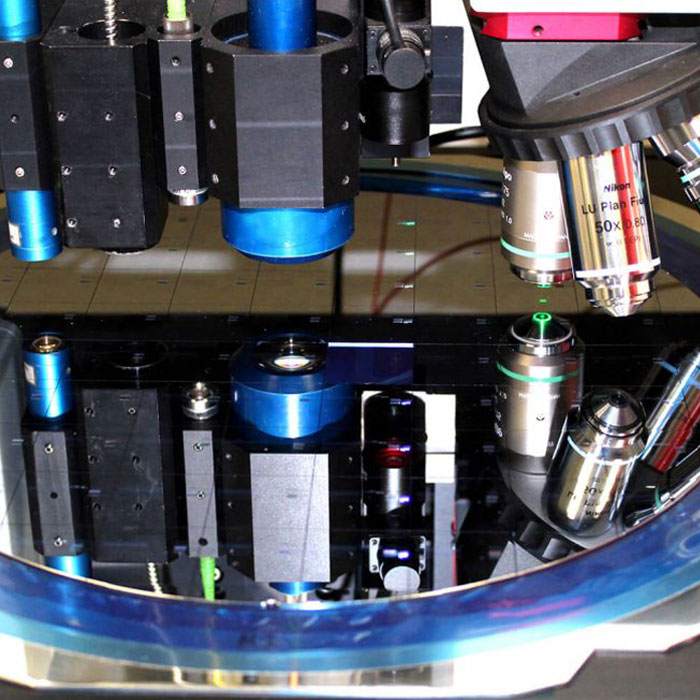
Optical Metrology and Inspection
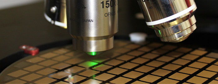
FRT Metrology tools uncover highly precise surface data to improve quality.
FRT Metrology manufactures powerful surface metrology tools for production, development, and quality control. Based on the design and construction of these multi-sensor devices, FRT Metrology tools can be used for a wide range of wafer and non-wafer applications.Fully Automated Wafer Metrology Tools
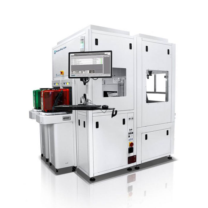
- The standard fully automated wafer metrology tools combine the capabilities of the worldwide established 300 mm metrology station, with a wafer handling system within an Equipment Front End Module (EFEM). With fully SEMI-compliant metrology solutions and robust hardware components, the MicroProf with EFEM is configurable for any front end high-volume fab, for a wide range of applications in the silicon wafer foundry, applications at different 3D packaging process steps, or comprehensive inspection applications.
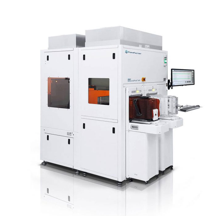

MicroProf® AP
-
Flexible Multi-sensor Metrology Tool for Advanced Packaging
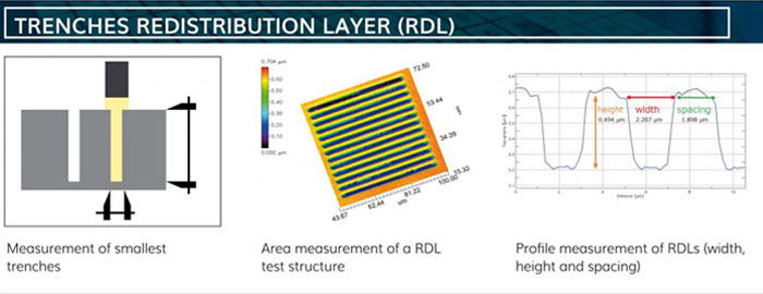
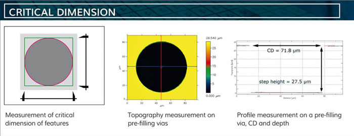
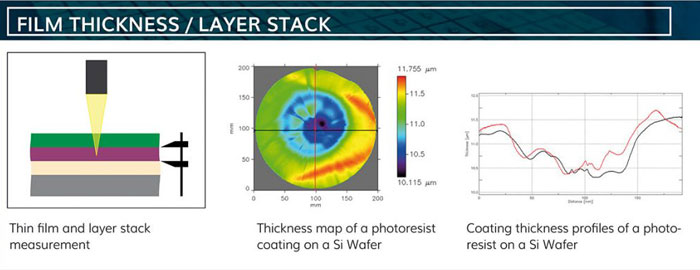
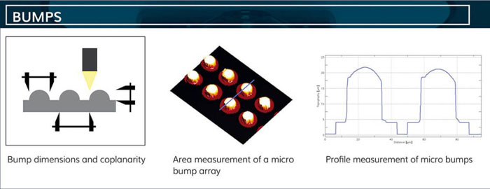
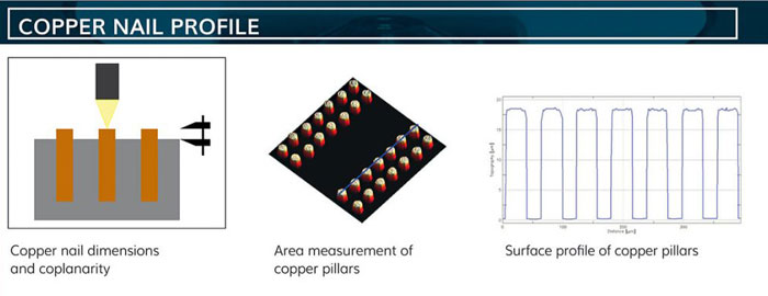
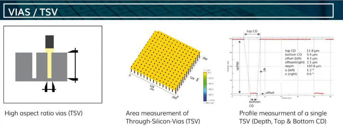
The FRT MicroProf® AP is a fully automated wafer metrology tool for a wide range of applications at different 3D packaging process steps, e.g. for the measurement of photoresist (PR) coatings and structuring, through silicon vias (TSVs) or trenches after etching, μ-bumps and Cu pillars, as well as for the measurement in thinning, bonding and stacking processes. With its modular multi-sensor concept, the flexible MicroProf AP measuring tool is ideally suited to perform a variety of measuring tasks in advanced packaging.
The FRT MicroProf AP also provides comprehensive measurement solutions for backside processing (backgrinding, metallization) for power semiconductors such as MOSFET or IGBT, as well as for the control of different substrates, e.g. bulk Si, SOI, cavity SOI, compounds such as GaAs, InP, SiC, GaN, ZnO, and also for transparent materials. Furthermore, it can be used for hybrid bonding and Micro Electro Mechanical Systems (MEMS), included in consumer electronics, automotive, telecom, medical and industrial markets.
Key Features- MicroProf AP Metrology System Flexible multi-sensor metrology tool for advanced packaging
- For every process step from TSV etching, RDL/UBM/bumping to Cu nail reveal, dicing, stacking, and molding
- Wafer handling unit with SEMI-standard FOUPs/FOSBs and open cassettes
- Individual configuration for your specific applications
- Retrofit on demand
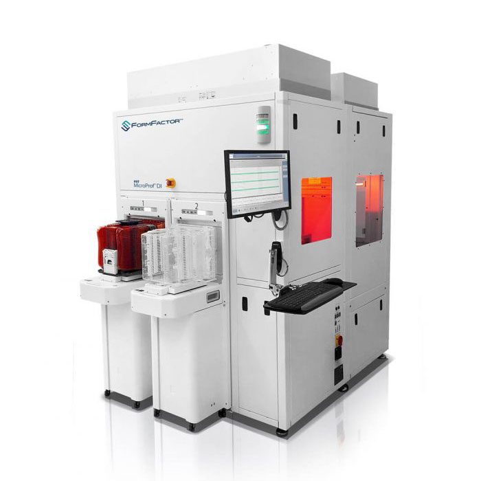
MicroProf® DI
- High-precision Optical Surface Inspection for Semiconductor Applications
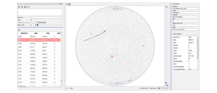
The FRT MicroProf DI optical inspection tool, enables inspection of structured and unstructured wafers during the entire manufacturing process. By combining 2D inspection and metrology, the MicroProf DI provides measurement solutions for a variety of applications, including defect inspection and wafer-level metrology for micro-bumps, RDL, overlay and through silicon via (TSV) in a single measuring tool.
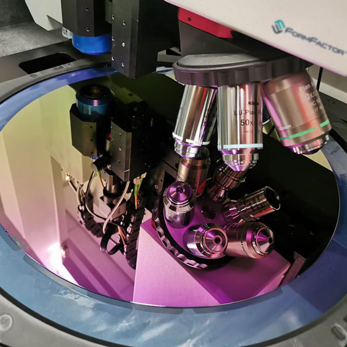
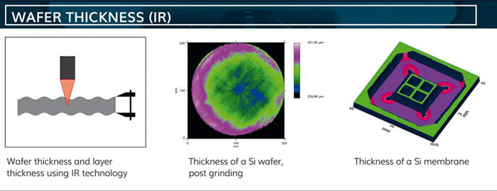
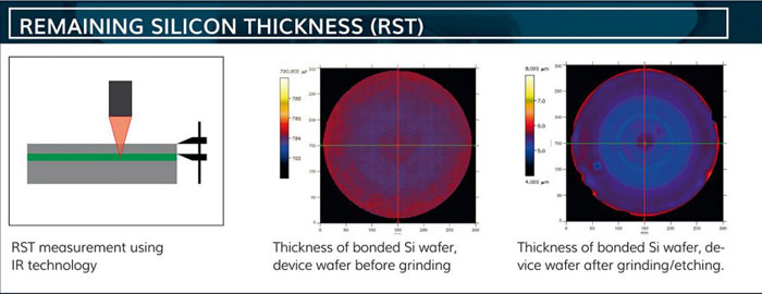
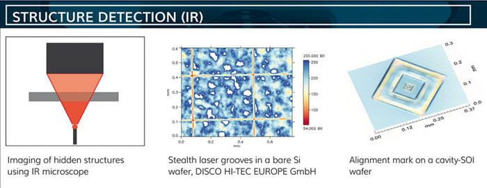
The MicroProf DI includes several modules that can be flexibly combined on the same tool platform, covering all wafer surfaces at high throughput for efficient process control. The modules include optical inspection and classification of defects via single-shot and step camera module, review of defects via a high-precision microscope and comprehensive multi-sensor metrology with different topography and layer thickness sensors. For the optical, non-contact and non-destructive analysis of hidden structures and inclusions in the wafer, interferometric layer thickness sensors with infrared light source and an IR microscope are also available.
Key Features- High-precision optical surface inspection for semiconductor applications
- Metrology and Inspection flexibly combined in one fully automated platform
- Defect inspection with single shot module, step camera and microscope station
- Fast and reliable inspection of defects down to sub-μm range
- Dark field micro inspection and bright field macro inspection
MicroProf® FE
- Fully Automated Metrology for Front-End Applications
The FRT MicroProf® FE is FormFactor’s standard, fully automated 2D/3D wafer metrology tool. It combines the capabilities of the established MicroProf 300 with a wafer handling system within an Equipment Front End Module (EFEM). With fully SEMI-compliant metrology solutions and almost maintenance-free hardware components, providing high throughput inspection, the MicroProf FE is the metrology solution in any front end HVM fab.
Besides the standard configuration, the FRT MicroProf FE can be equipped with numerous additional features, which can also be retrofit later.
Key Features- Fully automated 2D and 3D surface metrology for front-end applications
- Multi-sensor technology for hybrid metrology
- Specific inline solution for any high-volume manufacturing fab
- Single-arm robot unit for handling 300 mm (SEMI standard) wafers
- Vacuum end-effector handling
- 2 load ports for 300 mm FOUPs (SEMI standard)
- Optional pre-aligner and/or RFID reader
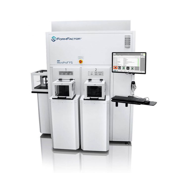
MicroProf® FS
- Multi-sensor Technology and Hybrid Metrology for MEMS and Foundries
The FRT MicroProf® FS is a fully automated wafer metrology tool, configurable for a wide range of applications in the wafer foundry, using both standard and customized solutions.
Flexibility and versatility are keywords when it comes to metrology solutions for today’s silicon foundry applications. MicroProf FS provides a modular approach to create a fully automated multi-sensor tool that can solve all required measurement tasks. That’s why we call it the Foundry Star!
For its core metrology component, the proven FRT MicroProf 300 multi-sensor metrology tool is used to allow the measurement of different products and – by using a hybrid metrology concept – enhances the precision of measurements on samples where a single sensor or measuring principle is just not enough. The measurement system of the MicroProf FS is equipped with a granite base setup, with a three-point sample fixture or a vacuum chuck.
Key Features- Fully automated multi-sensor technology and hybrid metrology setup for MEMS and Foundries
- Customizable for a wide range of applications within the Wafer Foundry
- Standardized hardware components integrated in customer-specific metrology solutions
- Handling of diverse substrate types
- Powerful inhouse software for fully automated 2D and 3D surface metrology
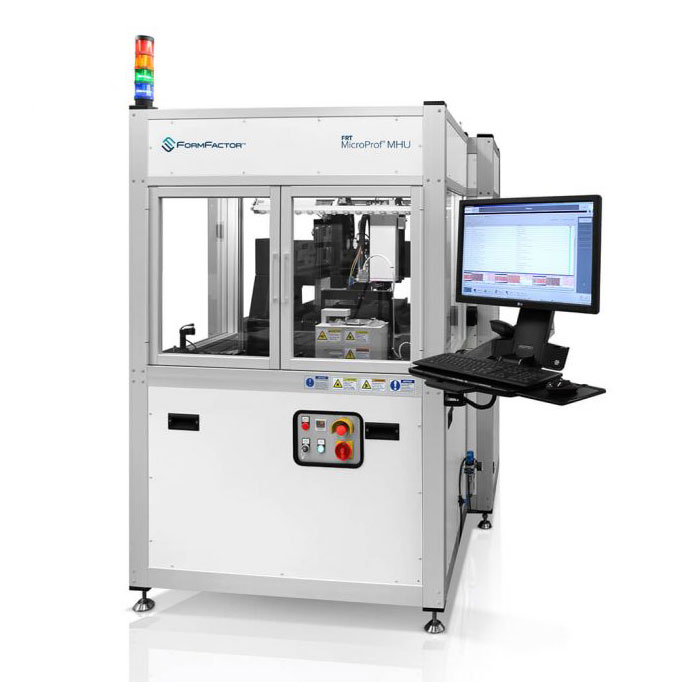
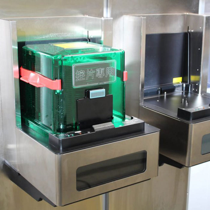
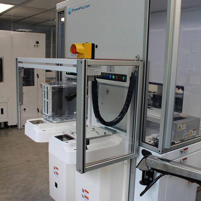
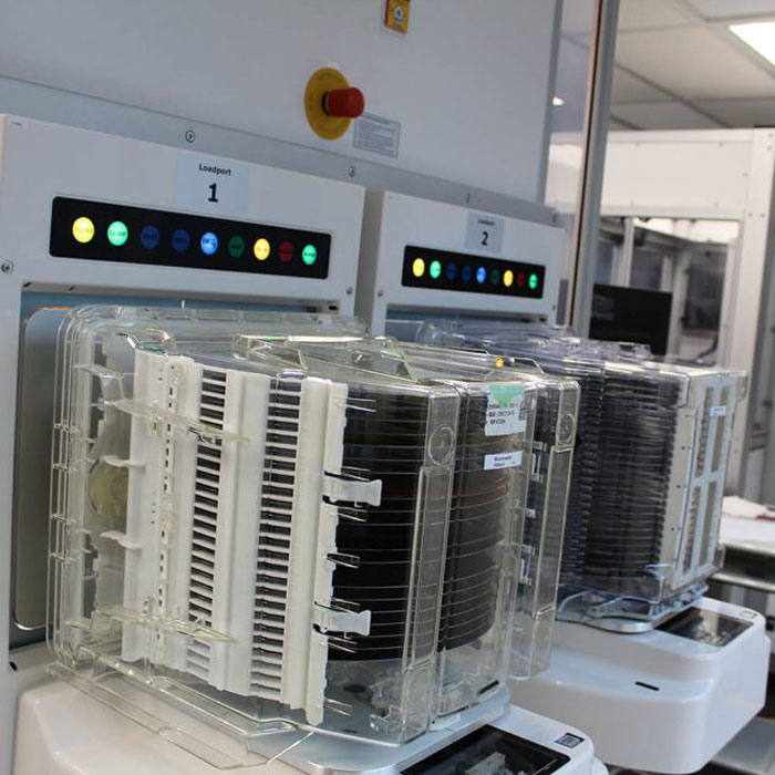
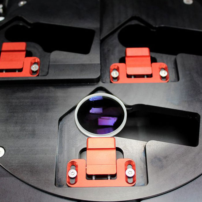
Semi-automated Metrology Tools with MHU
- The metrology tool with material handling unit is developed especially for the semiconductor, MEMS, sapphire, and LED industry. Typical applications are the measurement of bare, coated wafers and structured wafers in various lithographic process steps.
Due to a robotic arm with two vacuum end effectors, the device has a very high throughput of up to 220 wafers per hour. It can process wafer sizes from 2 to 8 inches. Up to 4 open cassettes can be processed and it is possible to integrate a pre-aligner and an OCR reader in the device. MicroProf® MHU
- Material Handling Unit with Dual-arm Robot for the Semiconductor, MEMS, and LED Industries
The FRT MicroProf® MHU metrology tool with Material Handling Unit, is specially designed for the semiconductor, MEMS, sapphire, and LED industries. Typical applications are measurements of bare and coated, as well as structured wafers at various lithographic process steps. Due to a robotic arm with two vacuum end effectors, the tool has very high throughput rates of up to 220 wafers per hour. It is capable of processing wafer sizes from 2 to 8 inches. Up to 4 open cassettes can be processed and, additionally, there is the option to integrate a pre-aligner and an OCR reader.
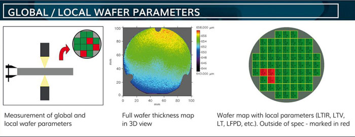
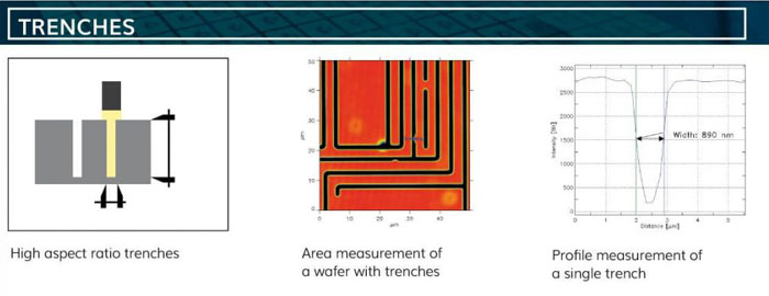
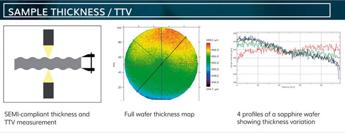
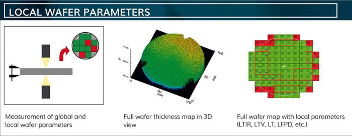
The option for two-sided sample measurement allows the simultaneous measurement of the top and bottom surface with determination of the sample thickness, total thickness variation (TTV) and various surface parameters such as roughness, waviness and flatness of both sides. A complete wafer shape measurement is also possible with analysis of the global and local wafer parameters. A wafer sorting function is available, which is adjustable according to customer requirements. Based on SurfaceSens technology, additional sensors can be retrofitted later. A further application of the MicroProf MHU is the layer thickness determination of thin films, as well as layer stacks, measurement of step heights, bumps, vias (TSVs), trenches, etc.
With its fully SEMI-compliant design, robust hardware components and high throughput, the FRT MicroProf MHU is the perfect metrology solution for production use.
Key Features- Material Handling Unit with dual arm vacuum grabber
- Optional edge handling and/or non-contact handling
- Different wafer sizes (from 2 up to 8 inches) in the same tool
- Optional OCR reader and pre-aligner
- Maximum flexibility thanks to multi-sensor setup
- Simultaneous measurement on both wafer sides (TTV)
- Fully automated recipe operation with FRT Acquire Automation XT software
- Optional SECS/GEM interface
- Sample sorting function, set up according to customer requirements
- Optional filter fan units, ISO class 4 clean room condition
Manual Metrology Tools
- High-precision optical surface metrology tools for the characterization of various functional and/or technical surfaces - fast, efficient, non-destructive.
Maximum flexibility is provided by the multi-sensor technology, developed by FormFactors FRT Metrology. It combines different measuring methods and sensors in one universally applicable tool of the MicroProf series - available as tabletop or stand-alone model depending on application and sample size - space-saving and upgradeable to your changing measurement requirements. 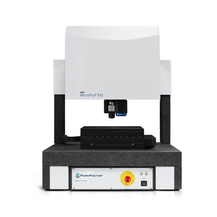
MicroProf® 100
- Multi-sensor Metrology Tool in a Table-top Unit
The FRT MicroProf® 100 is the universal surface metrology tool for quick and easy determination of topography, film thickness and sample thickness. As a compact table-top unit, and thus the smallest member of the MicroProf multi-sensor family, the MicroProf 100 offers the full flexibility of its bigger brothers. It is based on our proven SurfaceSens technology, in which different optical measurement methods – which otherwise can only be found in individual solutions– are merged into a universal and space-saving device.
In addition, the FRT MicroProf 100 can be equipped with the TTV option for double-sided sample inspection. This allows you to measure the top and bottom of the sample simultaneously and determine the sample thickness during the same measurement process. Due to its modular design, this metrology tool can be tailored to your specific application. In addition to the various sensors which can be added, the software can also be individually configured, and measurement tasks can be performed either manually or automatically.
Key Features- Tabletop unit with robust housing Based on the established FRT multi-sensor technology TTV option for double-sided sample inspection possible Integrated CCD camera with add-on illumination Motorized sensor approach with high-precision axis Simple and efficient control with FRT Acquire Software User-friendly FRT Mark III evaluation software with numerous evaluation and display options according to DIN-EN-ISO and SEMI standards Fully automated film thickness measurements through FRT Acquire Automation XT metrology software
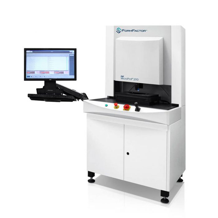
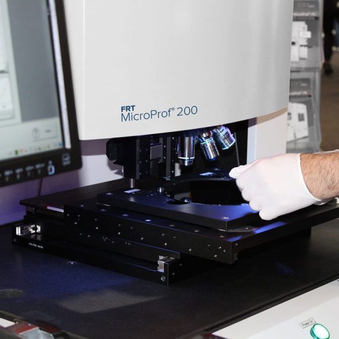
MicroProf® 200
- Universal Metrology Tool as Stand-alone Unit
The FRT MicroProf® 200 is a high-performance measuring device for contactless and non-destructive characterization of almost all surfaces and films. This surface measuring tool is based on our established SurfaceSens technology and can perform numerous measuring tasks within just one system. A high-resolution CWL sensor allows for easy and reliable measuring of many parameters, e.g. topography, roughness, and contour. With a wide range of additional sensors, it is also possible to adapt the MicroProf 200 individually to your measuring task. Using the TTV module for inspection from both sides or using the module for automatic sample handling (MHU), the MicroProf 200 can also be retrofitted easily to your new measurement requirements at any time. With these capabilities, the tool can meet the highest automation requirements.
Key Features- Full range of multi-sensor setups usable
- Integrated CCD camera with add-on illumination
- Control and measurement computer with TFT monitor
- Fast xy precision table with high motion and positioning accuracy
- Stable granite construction with excellent damping properties
- Simple and efficient control with FRT Acquire software
- Fully automated 2D and 3D measurements through FRTs Acquire Automation XT metrology software
- User-friendly FRT Mark III evaluation software with numerous evaluation and display options according to DIN-ISO and SEMI standards
MicroProf® 300
- Powerful Metrology Tool for Quality Assurance, Development and Manufacturing
The FRT MicroProf® 300 is part of the high-performance and versatile MicroProf generation and features our established SurfaceSens technology. The tool is particularly useful in quality assurance, development and manufacturing, where the smallest deviations from the ideal surface shape must be determined contact-free without destroying the sample, with surface precision down to the sub-μm range. Besides roughness of the sample surface, shape is one of the most important parameters. Narrow tolerances must be precisely determined. The FRT MicroProf 300 is perfect for these requirements and can also be integrated into fully automated production. An extensive range of sensors and the option of conducting double-sided sample inspections (TTV) make it possible to individual adapt the MicroProf 300 to suit your measuring task at any time. Furthermore, the simple automation of measurements boosts productivity and process reliability.
Key Features- Full range of multi-sensor setups usable
- Integrated CCD camera with add-on illumination
- Control and measurement computer with TFT monitor
- Motorized sensor approach with high-precision axis
- Vertical stitching function to expand the height measuring range
- Fast xy precision table with high motion and positioning accuracy
- Stable granite construction with excellent damping properties
- Simple and efficient control with FRT Acquire software
- Fully automated 2D and 3D measurements through FRTs Acquire Automation XT metrology software
- User-friendly FRT Mark III evaluation software with numerous evaluation and display options according to DIN-ISO and SEMI standards
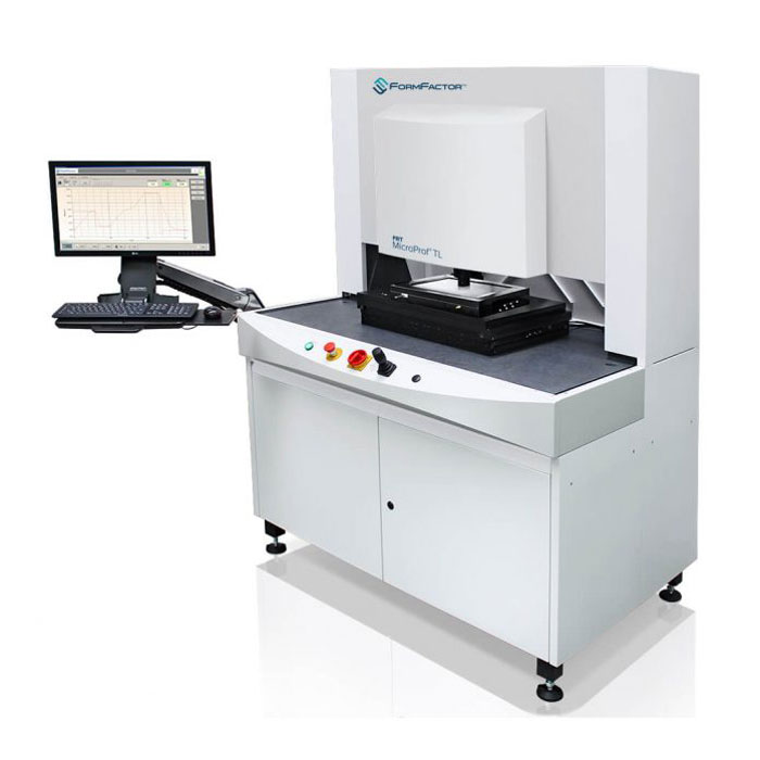
MicroProf® TL
- Optical Metrology with Programmable Temperature Control
The FRT MicroProf® TL is an optical surface measurement tool for fully automatic 3D surface measurements. Unique from other family members of the FRT MicroProf series, the TL features a Thermo Unit – a fully integrated heating and cooling stage – as well as a DLS deformation sensor by Chemnitzer Werkstoffmechanik. With these features, MicroProf TL can be used to characterize lateral and vertical deformation of samples under thermal load. This can be used to determine the behavior of components under working condition or to simulate various process steps. For the measurement process temperature cycles can be set as required by an easy recipe creation.
In combination with the software Acquire Automation XT, the MicroProf TL can run fully automatic temperature profiles. In the recipe, the user can set target temperatures, temperature ramps and dwell time that will be used during process. Set points can be defined where topography and deformation measurements take place within the heating/cooling process. Permanent temperature logging is available, and optionally, a second temperature probe can be added to monitor the temperature at special locations on the sample.
Key Features- Optical surface metrology tool with fully integrated heating and cooling stage
- Programmable temperature control from 10°C to 400°C
- High heating and cooling rate
- Temperature stability:
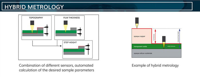
Metrology Software & Technology
- Our third generation platform including the multi-sensor concept combined with the complete in-house software empowers production lines around the world. Various metrology and inspection applications and surface parameters can be measured fully automated within one recipe and one tool.
SurfaceSens
- Modular optical metrology set-up for hybrid surface process control
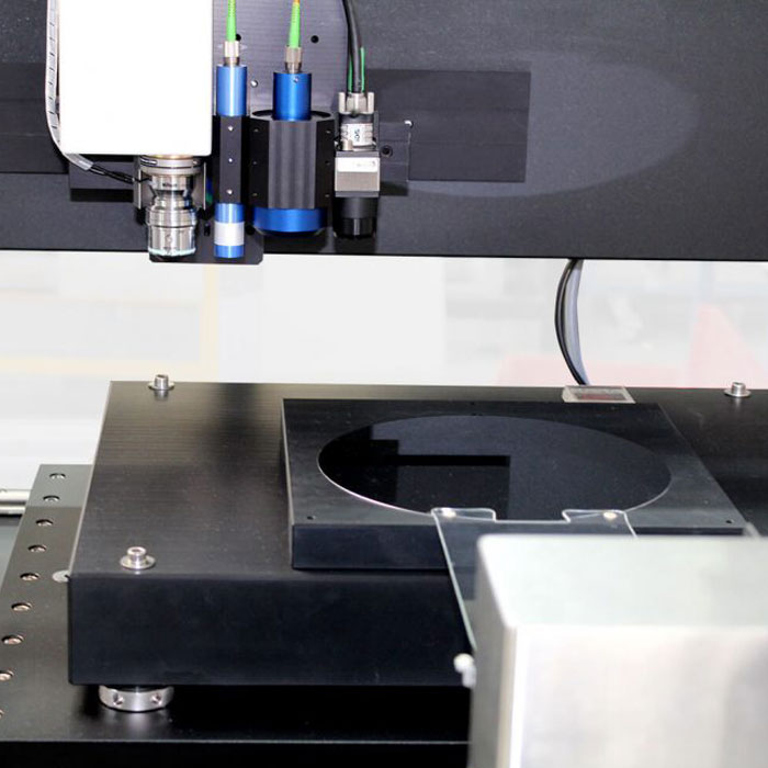
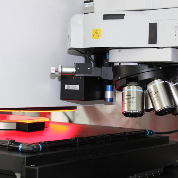
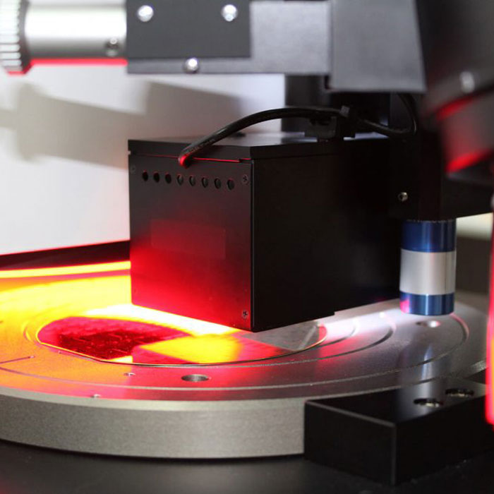
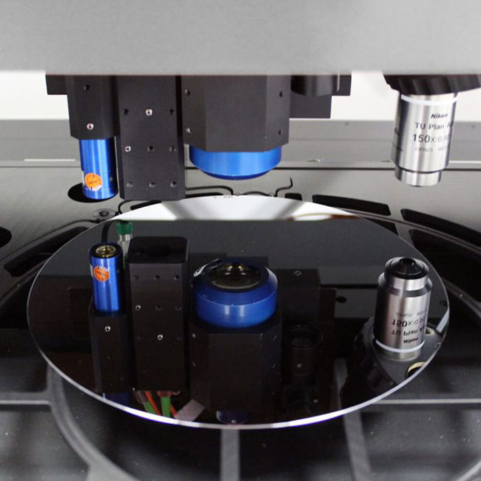
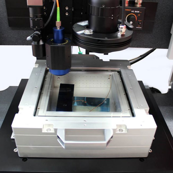
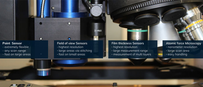
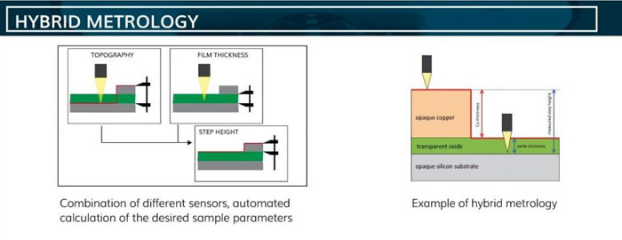
FormFactor's FRT Metrology engineers designed SurfaceSens technology to achieve superior information about the measured sample and greater insights about product quality. All of our FRT MicroProf® metrology tools can be configured with complementary sensor technologies. In a hybrid analysis process, otherwise inaccessible surface data of wafers or other samples are precisely measured.
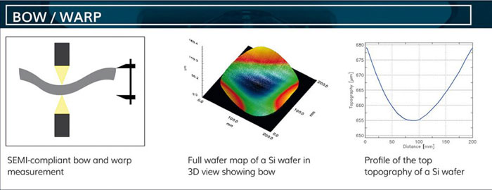
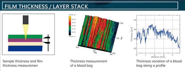
SurfaceSens offers you the possibility to combine unique metrology and inspection measuring principles in one single tool and thus allows maximum flexibility. The set-up, even for top and bottom sample measurement, with various optical sensors, like point, line and field of view sensors facilitates versatile results about several surface parameters, such as topography, roughness, TTV bow and warp, flatness, coplanarity, sample and layer thickness, and many others.
Retrofitting sensors opens further options for flexible adaptation to future measuring tasks, such as individual and exchangeable sample holders. You can solve your measurement tasks quickly, efficiently, and reliably - with FRT MicroProf plus SurfaceSens.

Mark III – Measurement Analysis Software
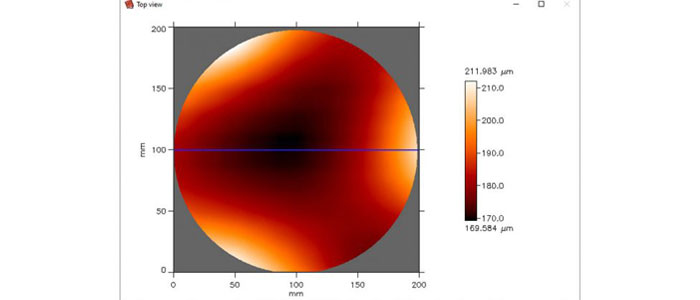
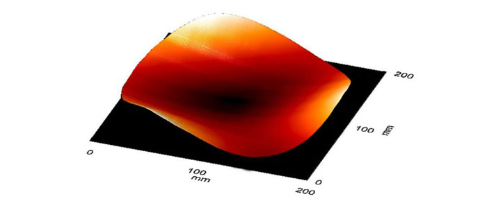
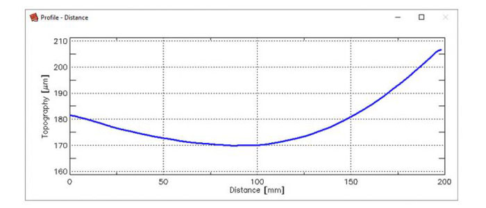
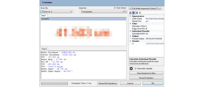
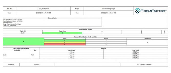
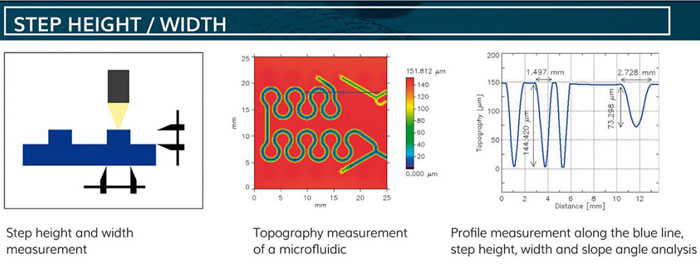
- The FRT Mark III analysis software is a comprehensive package for the processing, evaluation, and presentation of your 2D or 3D measurements. Latest standards like roughness and waviness calculation as well as many processing and filtering functions are implemented. Choose from a wide range of options, such as roughness, flatness, step height, layer thickness and many more, to select the analysis functions suitable for your application. Present your results in 3D, as profile view or top view and design your own measurement reports. This user-friendly software also has a wide range of import and export functions and can automatically perform several processing and evaluation steps on your measurement series.
Key Features
Analysis software for evaluation of surface and profile measurements- Evaluation of SPM data and other numerous import formats
- Determination of surface parameters according to international standards and guidelines (DIN EN ISO, SEMI, etc.)
- Various display options, e.g. 3D view, histogram, material fraction, autocorrelation
- Analysis of particles, pores and angles
- Extensive filter and modification functions
- Extraction of linear and curved profiles from area measurements
- Export of graphics, PDF measurement reports and other export formats
- Individually designable measurement protocol layouts
- Free updates
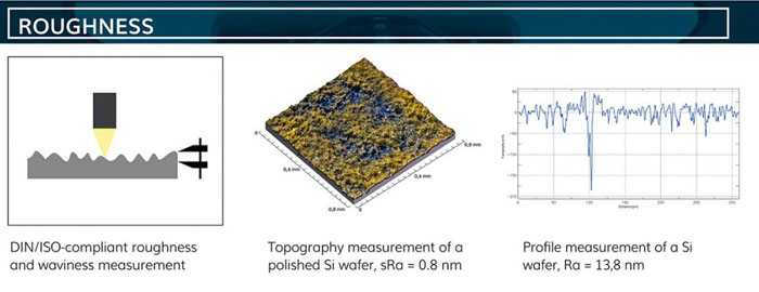
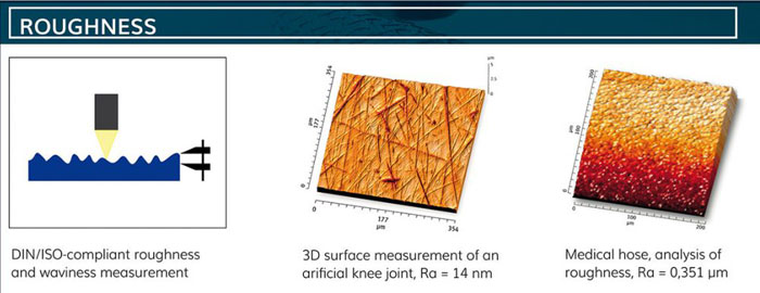
Roughness, waviness according to international standards and guidelines- Filtering and evaluation of profile and surface parameters according to DIN
- EN ISO 4287 and DIN EN ISO 25178
- Determination of waviness according to SEP 1941
- individual settings of all evaluation parameters possible
3D view- various shading methods
- freely selectable view and scaling
- large selection of color tables and user-defined colors
- 3D stereo display
Acquire Automation XT
- Easy recipe creation, multi-sensor measurement or hybrid metrology
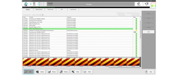
Acquire Automation XT is a fully automated software that carries out the measurement of components, the evaluation of measurement data and the logging of results. Easy recipe creation, multi-sensor measurement or hybrid metrology, compliance with industry standards or complex measurement tasks, are all standard in Acquire Automation XT. With the integration of different robot systems and interfaces for remote control, full integration into production is an easy step.
Key Features- Full automation of 2D and 3D measurements
- Selection of numerous measuring tasks, filters, and evaluations according to SEMI and DIN-EN-ISO standards
- Easy composition of individual measuring recipes with individual sample geometries and layouts
- Management of measurement results in database and export to various formats or direct transfer to a tracing system
- Integration of actuators such as robotic systems for sample handling and heating tables into the measuring sequence
- Seamless integration into production environments with interfaces for remote control such as SEMI SECS/GEM, iTAC
- Intuitive user interface with level-based user rights according to SEMI specifications
Applications and Industries
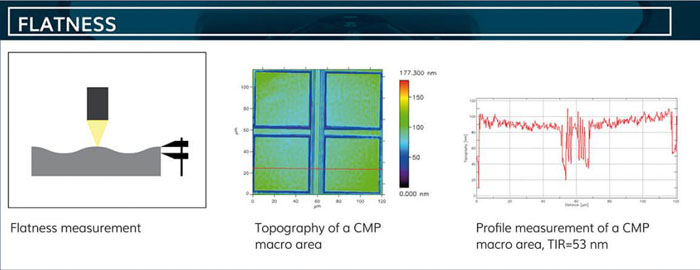
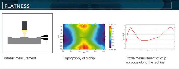

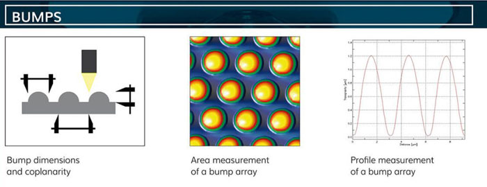
Advanced Packaging Applications
- Chip packaging techniques, including 2.5D, 3D-IC, fan-out wafer-level packaging and system-in-package, are all methods of advanced packaging. With advanced packaging, the need for flexibility in wafer metrology and handling has just exploded.
FRT Metrology Tools measure and handle numerous wafer types up to 12 inches for both front and back end: bare, structured, coated, bonded, highly warped, thinned, TAIKO and fan-out wafers, even wafers with Micro-Electronic-Mechanical components or at different 3D packaging process steps, but also glass, lens, and non-SEMI-standard wafers, panels and film frames.
The included dual arm robot handling unit can be configured for 300 mm, 200 mm, and 150 mm wafers and panels, both exclusive or as a bridge tool allowing the handling of two sample sizes within one metrology tool.
Our FRT MicroProf® AP system is specifically designed for metrology advanced packaging applications.
Our SurfaceSens multi-sensor technology, the modular based software and the retrofittable sensor hardware create the flexibility customers need in heterogeneous production cycles.
Semiconductor Applications
- Wafers are the substrate to manufacture semiconductors. Surface Metrology on wafers made of various conductive or non-conductive materials such as silicon, sapphire, or glass with a typical diameter of 100, 150, 200 or 300 mm is essential for quality assurance.
Manufacturers in the fields of semiconductor have high demands on the production tolerances of the pre-product “wafer”. Even small deviations can have a negative impact on the quality in the downstream, cost-intensive process steps.
High-quality, fully automated multi-sensor FRT Metrology technology contributes to the control of process tolerances in wafer manufacturing and helps to maintain the required quality standards of the producers.
Wafer measurement requires a high degree of precision. FRT Metrology tools measure and handle numerous wafer types up to 12 inches for both front and back end: Bare, structured, coated, bonded, highly warped, thinned, TAIKO and fan-out wafers, even wafers with Micro-Electronic-Mechanical components or at different 3D packaging process steps, but also glass, lens, and non-SEMI-standard wafers, panels and film frames.
The included dual arm robot handling unit can be configured for 300 mm, 200 mm, and 150 mm wafers and panels, both exclusive or as a bridge tool allowing the handling of two sample sizes within one metrology system.
Our SurfaceSens technology, the modular based software and the retrofittable sensor hardware create the flexibility customers need in heterogeneous production cycles.

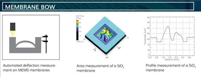

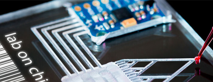
MST/MEMS/Nano Applications
- Mechanical parts and electronic circuits combine to form miniature devices, typically on a semiconductor chip, with dimensions from tens of micrometers to a few hundred micrometers. Common applications for MEMS include sensors, actuators, and process-control units. MEMS are the drivers of the IoT (Internet of Things).
Manufacturers in the fields of microelectronics and microsystems have high demands on the production tolerances of the pre-product “wafer”. Even small deviations can have a negative impact on the quality in the downstream, cost-intensive process steps.
Wafer measurement requires a high degree of precision. FRT Metrology Tools measure and handle numerous wafer types up to 12 inches for both front and back end: Bare, structured, coated, bonded, highly warped, thinned, TAIKO and fan-out wafers, even wafers with Micro-Electronic-Mechanical components or at different 3D packaging process steps, but also glass, lens, and non-SEMI-standard wafers, panels and film frames.
Our SurfaceSens technology, the modular based software and the retrofittable sensor hardware create the flexibility customers need in heterogeneous production cycles.
Sapphire LED Applications
- New LED and OLED technology designs are being developed. High-brightness light emitting diodes are (mostly) formed on sapphire wafers. The light extraction efficiency of the completed device will be drastically improved by very small structures patterned on the wafer.

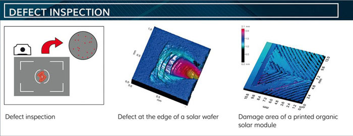
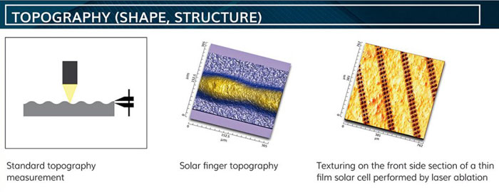
Photovoltaics Applications
- The sun as a direct energy source is growing in adoption worldwide. The application of solar technology is vital for smart grids, distributed power generation and the full participation of consumers in the energy market.
The high-volume PV manufacturing is fully automated. Anti-reflection coating thicknesses, as well as inspection of holes and scratches, metal contact layers, silver and aluminum paste and the printing of contact fingers are typical applications.
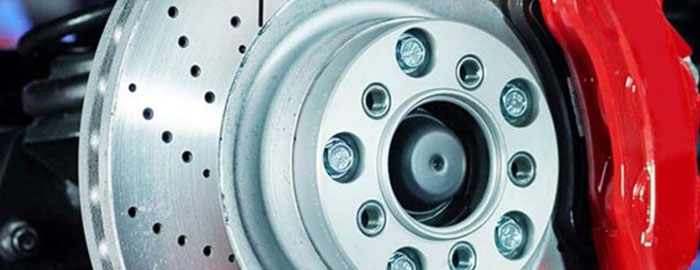
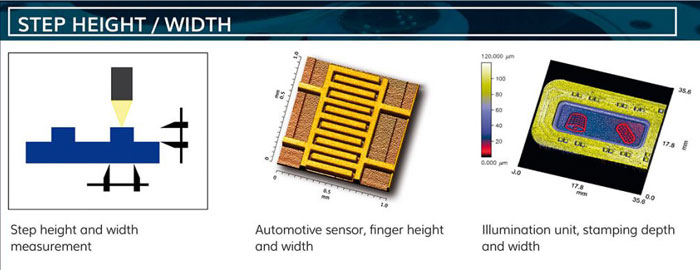

Automotive Applications
- The automotive industry is passing through disruptive times not only because of e-mobility. Inline (or near-line) production has even changed the demand for increased frequency in sampling and faster measurement and inspection time.
Advanced automobile manufacturers use automated metrology and include the created surface data into the management systems for its total product. Decisions about on-going production, thus ensuring that productivity is maintained, can be improved by the real-time intelligence of data.
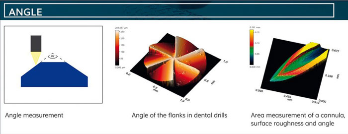
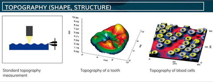
Medical Technology Applications
- In medical technology and biotechnology, the most innovative materials and technologies are combined. The durability and safety of these medical technology products are often used as quality factors. Everything must be right.
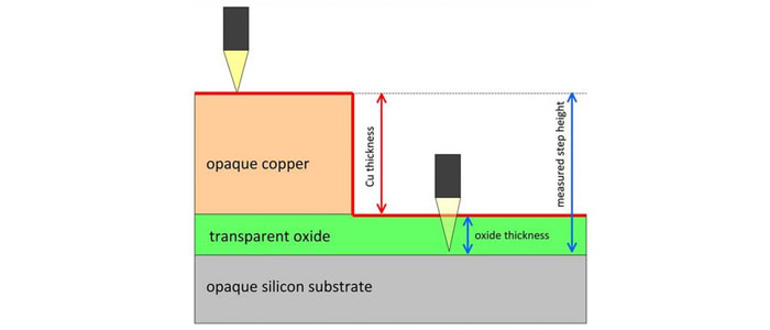
FRT Metrology tools measure roughness, film thickness, step heights or many other surface parameters.
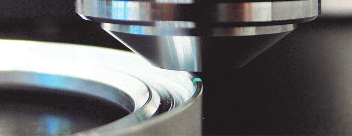
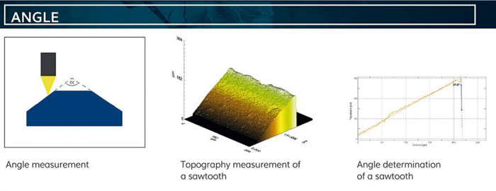

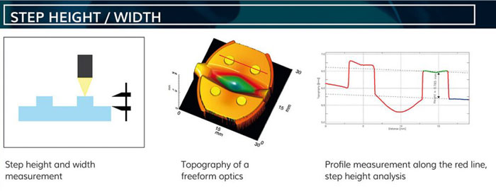
Engineering Applications
- Mechanical engineering is currently mastering Industry 4.0, yet the demand for ever more innovative and flexible solutions remains. Surface measurement technology in production engineering must be fast, accurate, robust, and automated, and ideally can be integrated into the production line.

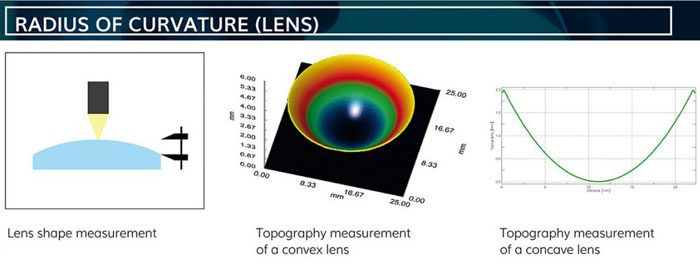

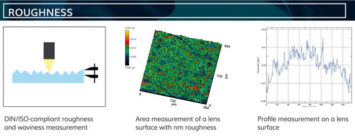
Optics Applications
- The surface quality of an optical lens describes its optical design and considers lens defects such as scratches, chipping, holes, or inclusions that have already penetrated the sub-nanometer range. These can reduce the optical throughput of the system and scatter diffused light.
Whether large lenses, lens arrays or micro-optics, optical systems and their manufacturing processes are becoming increasingly complex.


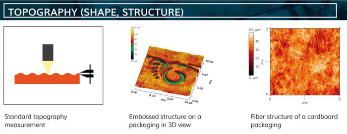
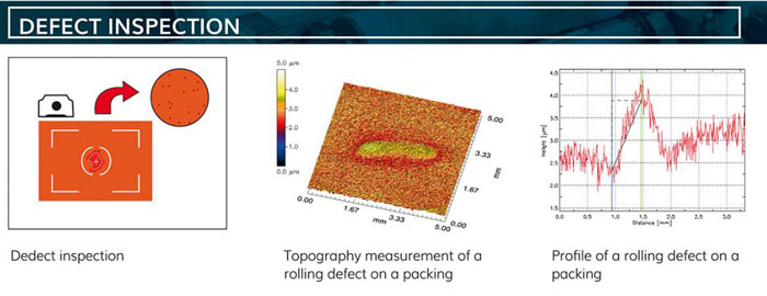
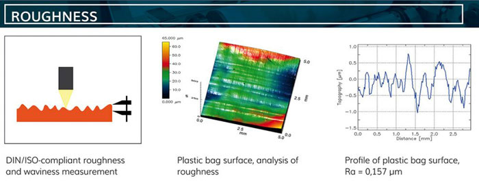
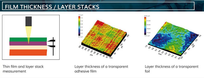
Packaging Applications
- Packaging that cannot be counterfeited is a proven means of product and brand protection. The surfaces are provided with special features, such as invisible inks. Surface measurement technology provides automation and individual adaptation in the analysis of these structures.
Product counterfeiting is particularly critical in the pharmaceutical sector. Their effects are sometimes hazardous to health or even life-threatening. Therefore, manufacturers are looking for ways to label their original products in such a way that the brand and consumers are protected.
The packaging design in the micro or nanometer range is an interesting option for counterfeit protection.