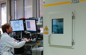
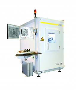
ESCATEC utilizes Nikon XT V 160 X-ray inspection system for more efficient detection

Photo by Nikon Metrology Europe NV
Swiss-owned electronic and mechatronic systems manufacturer, ESCATEC, has deployed a new X-ray inspection machine that sits alongside two lines producing printed circuit board assemblies (PCBA) at its factory in Heerbrugg. Supplied by Nikon Metrology, the XT V 160 machine is used for real-time, in-process quality control and replaces post-process X-ray inspection methodology. The in-line procedure is more efficient at detecting defects, has reduced the lead-time from order to delivery by one day, and optimizes costs by freeing an operator and a test engineer to be deployed elsewhere in the factory.
Dr Martin Muendlein, Engineering Manager at the ESCATEC plant, commented, “Modern electronic components are becoming smaller and smaller, increasing the need for sophisticated techniques to ensure that every solder joint is perfect.
“Visual inspection is increasingly difficult as more and more leads are hidden under the components, which means that the solder joints are only detectable by X-ray.
“Our latest Nikon XT V 160 X-ray inspection system, installed as part of a continuing process optimization program, enables us to look at hidden solder joints with an image resolution down to 1 micron. So we are ready to meet the increasingly stringent quality control requirements demanded by the miniaturization of electronics.”
Aimed mainly at the industrial and medical sectors, ESCATEC’s electronic systems are to be found in survey equipment, network analyzers, medical respirators and similar top-end instruments. Such systems contain advanced, high-density PCBAs including components such as ball grid arrays (BGA), quad-flat no-lead (QFN) interconnections, microchip carriers and fine pitch connectors.
Detection rates using the company’s two previous X-ray systems had fallen from 100 per cent to around 70 per cent over the past decade as the features of interest on PCBAs became smaller and more difficult to inspect. All boards produced were checked half a day or one day after they were manufactured to determine if they had passed or failed.
The Nikon Metrology equipment, with its ability to zoom in to x2,400 magnification, once again allows all features to be investigated, despite their smaller size. Its installation, on the factory floor, just a few meters from two SMT (surface mount technology) production lines, has also brought a fundamental change to quality control at Heerbrugg in that it is now an in-process rather than a post-process function.
Dr Muendlein continued, “Rather than trying to find every error produced on every board during SMT, we use the Nikon XT V 160 as a tool for verifying that the manufacturing process is operating at a high quality level.
“According to the defined sample rate, normally between 5 and 10 per cent, PCBAs are inspected and analyzed immediately after solder reflow. Findings are continuously fed back to the SMT lines to optimize production parameters. Results are stored in test logs for traceability.
“It has been a fundamental shift in our quality control procedures, whereby we monitor and manage the performance of the SMT lines, rather than find out a day later how many defective boards we have.
“Sporadic defects in hidden solder joints will not be detected by sample inspection but systematic defects are reduced by 20 per cent, which means we end up with more good boards.
“At the same time, delivery lead-times have been cut and the engineering effort needed for inspection has been reduced. We estimate that we now need one fewer full-time operator on X-ray inspection. Based on this saving and much lower test engineering effort, our investment in the Nikon equipment will be amortized in less than two years.”

Photo by Nikon Metrology Europe NV
The new inspection process
Total quality is the driving force behind ESCATEC’s market success. Manufacturing of PCBAs is complex and both SMT lines are changed over up to seven times per day on average. Batch size is typically between 50 and 100 boards. Only between 5 and 10 per cent of all possible PCBA defects, mainly lack of solder joint integrity or shorts under BGA’s, QFN’s, etc, are detectable by X-ray. Positioning and orientation of components on boards are inspected in-line on automatic optical inspection (AOI) machines that view all of the boards produced. The same team of inspection operators at Heerbrugg is in charge of both the 100 per cent optical inspection and sample X-ray quality control.
The latter is a semi-automatic process. More than 250 different PCBAs are produced at Heerbrugg, most of them double-sided. First, a program for each side is written to instruct the XT V 160 to run sequentially to all the spots of interest on the board. With a near-perfect example of any particular PCBA (golden board), a sample inspection protocol with reference images is created so that the operator is able to compare an actual image with the reference image. An ESCATEC operator visually appraises each feature and decides whether it passes or fails.
Purchasing decision
Two other ESCATEC production facilities, in Malaysia, first evaluated and installed Nikon Metrology XT V 160 X-ray machines. One has an image intensifier detector for checking boards of lower sophistication and the other a flat panel detector. The latter is capable of inspecting more complex, multi-layered boards and was the model chosen for Heerbrugg after further extensive trials.
A problem with ESCATEC Heerbrugg’s previous X-ray machines was that they were based on a different technology involving automated laminography and needed complex test programs written. The inspection process was carried out in two steps. First, all PCBAs were automatically inspected and separated into good boards and bad boards with suspected faulty solder joints. During the second step, an operator inspected the latter boards to verify which were good and which really contained faulty joints.
This type of machine is limited in that it can look at slices only from the top and bottom of the sample. There was no way to tilt the flat panel so that the operator could view the sample from the side. Additionally, the image resolution was not always sufficient for the decision process, especially for fine pitch BGAs, QFNs and similar. It is very difficult to see certain defects from one end of a PCBA, such as a BGA solder joint defect known as head-in-pillow. It is of major concern in the electronics industry, as the joint may have electrical integrity in the beginning but insufficient mechanical strength, making it prone to failure in the field, leading to costly repairs.
The ability of the XT V 160′s flat panel to tilt the sample by up to 60 degrees, combined with variable magnification, allows head-in-pillow and other defects to be seen easily by the operator. A further advantage is the open tube design, allowing simple replacement of the 160 kV / 20 W filament source, unlike on the former X-ray machine which had a closed tube. It was also temperamental, leading to high maintenance costs. Dr Muendlein states that the Nikon Metrology machine costs much less to maintain and to run.
When reviewing the market for its new X-ray facility, the team at Heerbrugg considered a number of different potential suppliers. They decided that the XT V 160 was the best fit for their application, as its cost-to-performance ratio was better than that of the other machines evaluated.
For more information, please visit http://www.nikonmetrology.com.
News Categories
- » NEWS HOME
- » Automation & Robotics
- » Industry 4.0
- » Material Handling
- » Sensors
- » Quality & Testing
- » Machine Vision
- » Laser & Optics
- » Metalworking
- » Motion Control & Drives
- » Hydraulics & Pneumatics
- » Process Industry
- » Renewable Energy
- » Agriculture
- » Home & Office Furniture
- » Additive Manufacturing
- » Environmental Tech

