Mitsubishi Electric’s new high-speed contact image sensor showcased at VISION 2016
Mitsubishi Electric has responded to the needs of the surface inspection market, in particular within the print industry, with the launch of a high-speed version of its Mitsubishi Electric Line Scan Bar, contact image sensor (CIS).
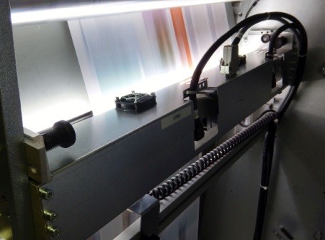
Photo by Hunkeler AG
The new high-speed contact image sensor (CIS) offers a compact, distortion-free alternative to line scan cameras. It was featured on the Stemmer Imaging GmbH exhibition at VISION 2016 in Stuttgart and supported by Mitsubishi Electric representatives at the show.
Mitsubishi Electric has responded to the needs of the surface inspection market, with the launch of a high-speed version of its contact image sensor (CIS), distributed under the name Mitsubishi Electric Line Scan Bar. Offering high quality, distortion-free image acquisition right up to the edges of the material, the new CIS scans surfaces at speeds up to 1000m per minute and above, in a compact, easy to install format.
For all machine builders, system integrators and end users, the CIS offers an ideal alternative to line scan cameras for inspecting defects on flat surfaces. Compared with a line scan camera, the CIS is simple to install, held in place directly above the surface of interest at a fixed height, with all LED illumination and optics built in. Mitsubishi Electric estimates that, with just four screws and four cables, the CIS can be installed in just a few minutes, compared with the hours or even days that might be required to install and align a line scan camera system with its complex set-up and numerous ancillaries.
By being close to the material instead of mounted high above, the CIS also helps to significantly reduce the overall footprint, and therefore the costs and complexity of the machine. Ease of installation and removal means maintenance and support requirements are also significantly reduced. This benefits not only machine builders but also end users who now no longer need to have specialist engineers on standby and can be assured of minimal downtime in the event of a problem.
Typical application areas for the CIS include the print and thin film production industries, where it can be used to detect surface defects on paper, plastics, fabrics, banknotes and even holograms. The CIS is available in a range of widths that match the most common sizes, and for larger material widths multiple CIS sensors can be cascaded side-by-side with seamless image acquisition right across the full width of the material. The CIS can also be used for the surface inspection of wood, glass and other materials. In addition, the CIS can form the heart of an automated optical inspection system for circuit boards.
Markus Köhler, Mitsubishi Electric Business Development Manager, comments: “The new CIS offers high quality image acquisition in the smallest footprint ever. Taking up so little space, and with its ease of installation and integration, the CIS is a solution that all machine builders, system integrators and end users have been waiting for. By addressing the widely appreciated challenges associated with using line scan cameras we have a potentially popular, game changing solution. With guaranteed distortion-free image acquisition right up to the edges of the material, and no need to sacrifice resolution for larger material widths – as you would have to with a line scan sensor. The CIS improves both defect detection and machine throughput; with this new high-speed version, we can match any line scan camera system for headline performance.”
This latest development from Mitsubishi Electric will be supported in the European markets by Stemmer Imaging, which is the preferred distributor for the contact image sensor.
For more information, please visit http://eu3a.mitsubishielectric.com.
News Categories
- » NEWS HOME
- » Automation & Robotics
- » Industry 4.0
- » Material Handling
- » Sensors
- » Quality & Testing
- » Machine Vision
- » Laser & Optics
- » Metalworking
- » Motion Control & Drives
- » Hydraulics & Pneumatics
- » Process Industry
- » Renewable Energy
- » Agriculture
- » Home & Office Furniture
- » Additive Manufacturing
- » Environmental Tech
Related Expos


Tags
|
|
|
|
|
|
|
|
|
|
|
|
|
|