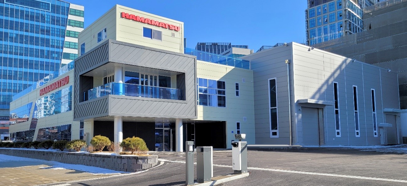
HAMAMATSU PHOTONICS KOREA has recenty completed new factory
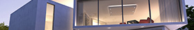
HAMAMATSU PHOTONICS KOREA Co., Ltd., a Korean subsidiary of Hamamatsu Photonics K.K., has completed construction of a new factory in Hwaseong-si, Gyeonggi-do, Republic of Korea (hereafter South Korea). This new factory will boost its production capacity of semiconductor failure analysis equipment and expand its sales in the global market. The manufacturing plant will be moved from the current factory to this new factory, and full-scale operations will begin in March 2025.
In March 2020, we established HAMAMATSU PHOTONICS KOREA Co., Ltd. as a Korean subsidiary to manufacture semiconductor failure analysis equipment and promote sales of image measurement equipment in South Korea. This subsidiary has contributed to expanding our image measurement equipment business there. In the field of semiconductor failure analysis, we have accurately grasped the needs of our customers, including Korean semiconductor manufacturers, and developed new technologies to meet those needs. As a result, our semiconductor failure analysis equipment maintains a high global market share .
The recent spread of generative AI is driving a surge in demand for state-of-the-art semiconductors. Dealing with this demand requires early yield improvement in the ongoing development of high-performance memory and logic devices. This has also led to an increased need for semiconductor failure analysis, and equipment with automation capabilities is required to analyze huge numbers of devices quickly.
There are two types of automation functions for semiconductor failure analysis. The first function automatically switches the observation viewpoint from low to high magnification. This allows rapidly pinpointing and identifying failure locations. The second function speedily inspects the entire wafer to detect process abnormalities at an early stage. This enables early detection of abnormalities in the manufacturing process and in this way contributes to improving the product yield. We are developing equipment with these two types of automation functions.
Starting up this new factory will boost our ability to meet many market needs, including the development, manufacture, and demonstration of semiconductor failure analysis equipment. The new factory will also serve as a commercial distribution point for our electron tube and optosemiconductor products when importing, storing, and selling these in the South Korean market.
For more information visit: hamamatsu.com
News Categories
- » NEWS HOME
- » Automation & Robotics
- » Industry 4.0
- » Material Handling
- » Sensors
- » Quality & Testing
- » Machine Vision
- » Laser & Optics
- » Metalworking
- » Motion Control & Drives
- » Hydraulics & Pneumatics
- » Process Industry
- » Renewable Energy
- » Agriculture
- » Home & Office Furniture
- » Additive Manufacturing
- » Environmental Tech
Related Expos


Tags
|
|
|
|
|
|
|
||
|
|
|
|
|
|
|
|
|